Soi device and method for its fabrication

a technology of semiconductor devices and dielectric materials, applied in semiconductor devices, diodes, electrical apparatus, etc., can solve problems such as destructive discharge through capacitor dielectric materials, significant voltage spikes on bus, and affecting the yield and reliability of integrated circuits

Inactive Publication Date: 2008-01-24
GLOBALFOUNDRIES US INC
View PDF8 Cites 41 Cited by
  • Summary
  • Abstract
  • Description
  • Claims
  • Application Information

AI Technical Summary

Problems solved by technology

Especially as the switching speed of the integrated circuits increases, the requirement of sourcing or sinking current by a bus can cause significant voltage spikes on the bus because of the inherent inductance of the bus.
One problem that can affect the yield and reliability of the integrated circuit can occur when using such MOS capacitors as the decoupling capacitors between voltage busses.
The problem occurs because sufficient charge can build up on a capacitor during fabrication of the IC to cause a destructive discharge through the capacitor dielectric material.
This problem becomes more severe as device sizes shrink and especially as the thickness of the gate dielectric layer is reduced.

Method used


Image

  • Soi device and method for its fabrication
  • Soi device and method for its fabrication
  • Soi device and method for its fabrication

Examples


Embodiment Construction

[0011]The following detailed description is merely exemplary in nature and is not intended to limit the invention or the application and uses of the invention. Furthermore, there is no intention to be bound by any expressed or implied theory presented in the preceding technical field, background, brief summary or the following detailed description.

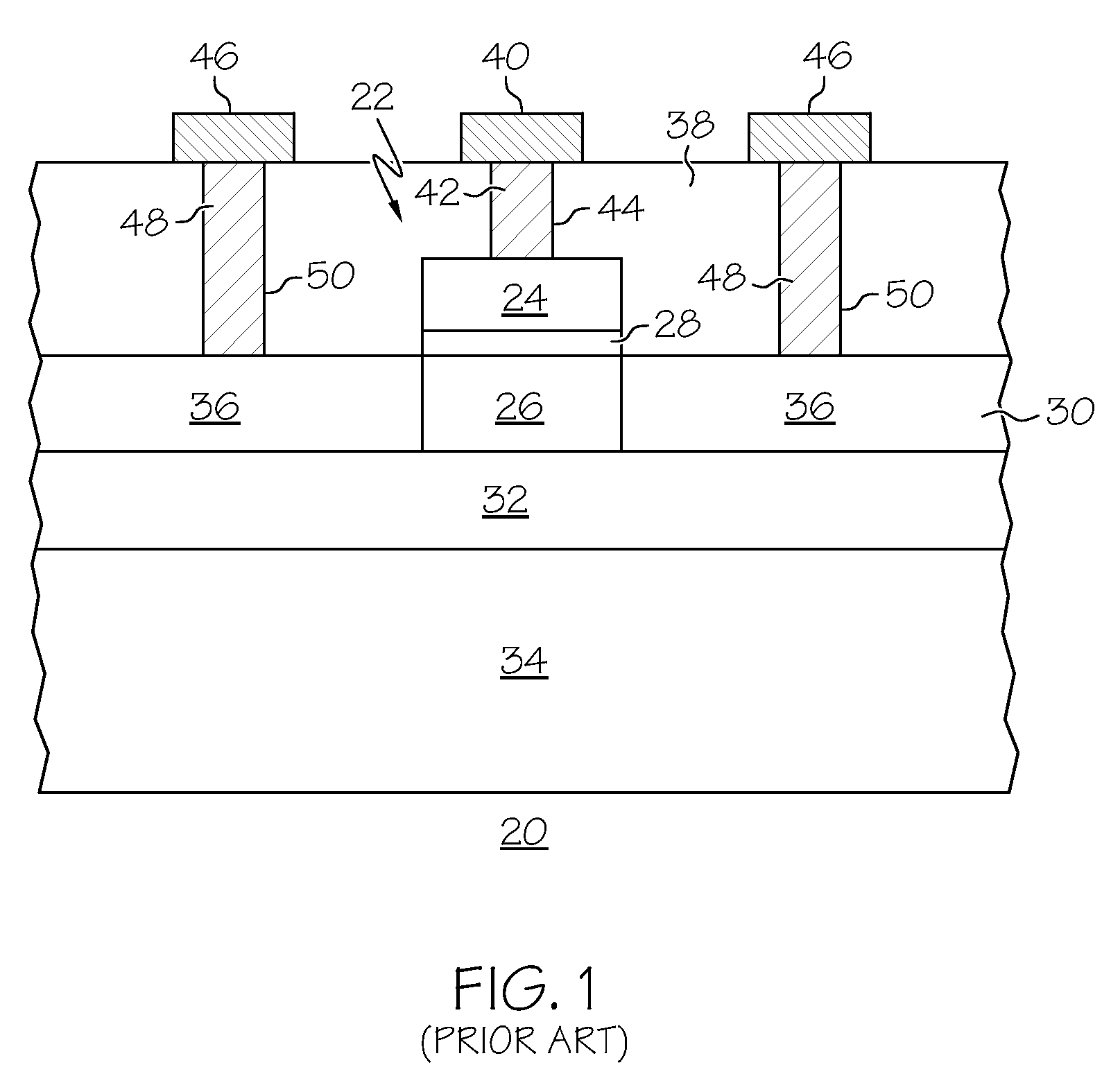
[0012]FIG. 1 illustrates, in partial cross section, elements of a conventional decoupling capacitor structure 20 implemented in a portion of a silicon on insulator (SOI) integrated circuit (IC) device structure. Such an IC structure might include a plurality of distributed MOS capacitors 22 (only one of which is illustrated), each of which includes a top plate 24, a bottom plate 26 and a capacitor dielectric 28. Top plate 24 generally is formed from the same material as are the gate electrodes of the MOS transistor that make up the remainder of the IC. Capacitor dielectric 28 generally is formed of the same material used for the gate diele...


PUM


Abstract

A silicon on insulator (SOI) device and methods for fabricating such a device are provided. The device includes an MOS capacitor coupled between voltage busses and formed in a monocrystalline semiconductor layer overlying an insulator layer and a semiconductor substrate. The device includes at least one electrical discharge path for discharging potentially harmful charge build up on the MOS capacitor. The MOS capacitor has a conductive electrode material forming a first plate of the MOS capacitor and an impurity doped region in the monocrystalline silicon layer beneath the conductive electrode material forming a second plate. A first voltage bus is coupled to the first plate of the capacitor and to an electrical discharge path through a diode formed in the semiconductor substrate and a second voltage bus is coupled to the second plate of the capacitor.

Description

TECHNICAL FIELD[0001]The present invention generally relates to a semiconductor on insulator (SOI) device and to methods for fabricating such a device, and more particularly to SOI devices and to methods for fabricating SOI devices including a discharge path for a decoupling capacitor.BACKGROUND[0002]The majority of present day integrated circuits (ICs) are implemented by using a plurality of interconnected field effect transistors (FETs), also called metal oxide semiconductor field effect transistors (MOSFETs or MOS transistors). The ICs are usually formed using both P-channel FETs (PMOS transistors or PFETs) and N-channel FETs (NMOS transistors or NFETs) and the IC is then referred to as a complementary MOS or CMOS circuit. Certain improvements in performance of MOS ICs can be realized by forming the MOS transistors in a thin layer of semiconductor material overlying an insulator layer. Such semiconductor on insulator (SOI) MOS transistors, for example, exhibit lower junction capa...

Claims


Application Information

Patent Timeline
Patent Type & Authority Applications(United States)
IPC IPC(8): H01L29/76H01L21/8238
CPCH01L21/84H01L27/1203H01L27/0255H01L21/743H01L27/02H01L27/04H01L27/12
Inventor PELELLA, MARIO M.WU, DONGGANG D.BULLER, JAMES F.
Owner GLOBALFOUNDRIES US INC
Why Eureka
Try Eureka