Liquid crystal display device and a manufacturing method of the same

a technology of liquid crystal display and manufacturing method, which is applied in the direction of static indicating devices, operating means/releasing devices of valves, instruments, etc., can solve problems affecting quality or yield, and achieve the effect of preventing an increase in the number of photo-etching processes

Active Publication Date: 2008-01-24
OPTRONIC SCI LLC
View PDF5 Cites 0 Cited by
  • Summary
  • Abstract
  • Description
  • Claims
  • Application Information

AI Technical Summary

Benefits of technology

[0037] In the liquid crystal display device described above in the present invention, an insulating gate-type transistor has a protective insulating layer on the channel, so a passivation function is provided by selectively forming a photosensitive organic insulating layer only on source-drain wires in an image display area or only on the signal line or by anodizing the source-drain wires comprising anodizable source-drain material and forming an insulating layer on the surfaces of the source-drain wires. Because of this, an exceptionally heating process is not used, so excess heat resistance is not required in the insulating gate-type transistor made in which an amorphous silicon layer is used as a semiconductor layer. To put it another way, effects are added wherein the electrical performance does not deteriorate in the formation of passivation. Also, in the anodization of the source-drain wires, it is possible to selectively protect the tops of electrode terminals for the scan line and the signal line by introducing half-tone exposure technology, obtaining the effect of preventing an increase in the number of photo-etching processes.
[0038] Additionally, the formation process of pixel electrodes is streamlined by forming pseudo-pixel electrodes and scan lines comprising a laminate made of a transparent conductive layer and a first metal layer, and removing the first metal layer from the top of the pseudo-pixel electrodes during the formation of contacts (openings) on the pseudo-pixel electrodes to obtain transparent conductive pixel electrodes. As a result, a four-mask process without concomitant use of half-tone exposure technology is achieved unlike a conventional four-mask process with concomitant use of half-tone exposure technology, simplifying channel length management.
[0039] Also, by using half-tone exposure technology with a lower pattern accuracy during the formation of the source-drain wires, it is possible to obtain electrodes for the signal line and the scan line comprising a metal layer, so variety can be provided in the device.
[0040] Further, coupled with the process reduction where the formation process of protective insulating layers (etch-stop layers) and the formation process of openings (contacts formation process) in the gate insulating layer with one photomask is made possible by introducing half-tone exposure technology, the number of photo-etching processes is further decreased from five photomasks, making it possible to produce a liquid crystal display device using four or three photomasks. This is the result of decreasing the number of manufacturing processes of the active substrate, and is the greatest feature from the perspective of decreasing costs of the overall liquid crystal display device. Moreover, the pattern precision of these processes is not so high, so controlling production without greatly affecting quality or yield is an easy matter.
[0041] An electric field generated between the counter electrode and the pixel electrode in an IPS-type liquid crystal display device according to Embodiments 11 and 13 is applied only to the gate insulating layer, and an electric field generated between the counter electrode and the pixel electrode in an IPS-liquid crystal display device according to Embodiments 12 and 14 is applied to the gate insulating layer and the anodized layer of the pixel electrode, so a conventional inferior passivation insulating layer with many defects is not used, and the advantage of the rarity of the display image sticking phenomenon is enjoyed. The reason for this is that no charge accumulates due to the anodized layer of the drain wire (pixel electrode) functions as a high resistance layer rather than an insulating layer.

Problems solved by technology

Moreover, the pattern precision of these processes is not so high, so controlling production without greatly affecting quality or yield is an easy matter.

Method used


Image

  • Liquid crystal display device and a manufacturing method of the same
  • Liquid crystal display device and a manufacturing method of the same
  • Liquid crystal display device and a manufacturing method of the same

Examples


embodiment 1

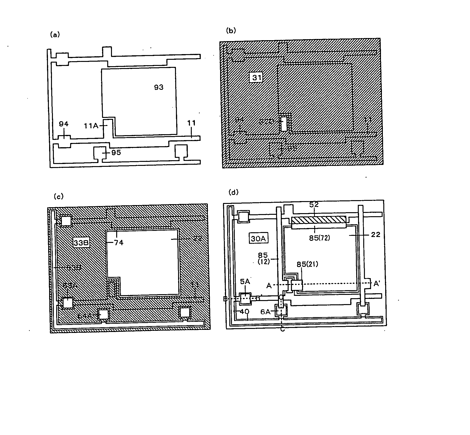
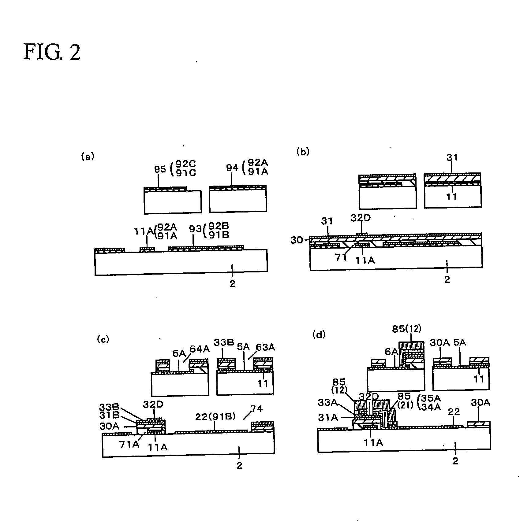
[0080] In Embodiment 1, first, an SPT or other vacuum film depositing equipment is used to deposit ITO, for example, as a transparent conductive layer 91 about 0.1 to 0.2 μm thick and a first metal layer 92 about 0.1 to 0.3 μm thick on the main surface of glass substrate 2. Then, scan lines 11 doubling as gate electrodes 11A comprising a laminate made of a transparent conductive layer 91A and first metal layer 92A and pseudo-electrode terminals 94 of the scan lines; pseudo-pixel electrodes 93 comprising a laminate made of a transparent conductive layer 91B and a first metal layer 92B; and pseudo-electrode terminals 95 of signal lines comprising a laminate made of a transparent conductive layer 91C and a first metal layer 92C, are selectively formed using photosensitive resin patterns using micro-fabrication technology as shown in FIG. 1 (a) and Figure (2). A metal with a high melting point such as Cr, Ta, or Mo, for example, or an alloy or a silicide thereof may be selected for the ...

embodiment 2

[0087] In Embodiment 2, the process proceeds nearly identically to that in Embodiment 1 up until the contact formation process as shown in FIG. 3(c) and FIG. 4(c). Because of the reason described below, the pseudo-electrode terminal and 95 of the signal line and are not necessarily required. A thin film layer 34 of Ti, Ta, or the like, for example, is deposited about 0.1 μm thick as a heat-resistant metal layer, and then an Al thin film layer 35 is subsequently deposited as a low-resistance wire layer about 0.3 μm thick using an SPT or other vacuum film depositing equipment in the source-drain wires formation process. Then, the source-drain wire materials comprising these two thin film layers, the second amorphous silicon layer 33B, and the first amorphous silicon layer 31B are successively etched using the photosensitive organic insulating layer patterns 86A and 86B, using micro-fabrication technology to expose the protective insulating layers 32D and the gate insulating layer 30A ...

embodiment 3

[0094] In Embodiment 3, a process nearly identical to that in Embodiment 2 is carried out until where openings 63A are formed on part of the scan lines 11 outside the image display area to expose part of the scan lines 11 as shown in FIG. 5(c) and FIG. 6(c). Continuing, a thin film layer 34 of Ti, Ta, or the like, for example, is deposited about 0.1 μm thick as an anodizable heat-resistant metal layer, and then an Al thin film layer 35 is similarly deposited as an anodizable low-resistance wire layer about 0.3 μm thick using an SPT or other vacuum film depositing equipment in the source-drain wire formation process. Then, source-drain wire materials comprising these two thin film layers, the second amorphous silicon layer 33B, and the first amorphous silicon layer 31B are successively etched using the photosensitive resin patterns 87A and 87B using micro-fabrication technology to expose the protective insulating layers 32D and the gate insulating layer 30A. The drain electrodes 21 o...


PUM

PropertyMeasurementUnit
photosensitiveaaaaaaaaaa
lengthaaaaaaaaaa
dimensionaaaaaaaaaa

Abstract

A four-mask process and a three-mask process proposal are constructed for a TN-type liquid crystal display device and an IPS-type liquid crystal device in which the formation of a passivation insulating layer is not required by streamlining the formation of a scan line and a pseudo-pixel element, both comprising a laminate made of a transparent conductive layer and a metal layer, at the same time and the formation of the transparent conductive pixel electrode by removing the metal layer on the pseudo-pixel electrode at the time of the formation of the opening in the gate insulating layer, by streamlining the treatment of the formation process of the contact and the formation process of the protective insulating layer using one photomask due to the introduction of half-tone exposure technology, and the formation of source-drain wires for etch-stop type insulating gate-type transistor using a photosensitive organic insulating layer and leaving the photosensitive organic insulating layer unchanged on source-drain wires or on the source wire (signal line), or by forming an anodized layer, which is an insulating layer, on source-drain wires.

Description

FIELD OF THE INVENTION [0001] The present invention relates to a liquid crystal display device with a color image display function, and in particular to an active-type liquid crystal display device. DESCRIPTION OF THE RELATED ART [0002] Televisions and various other image display devices that have a liquid crystal display 5 to 50 cm in diagonal length are commercially available in mass quantity through the progress in recent years in micro-fabrication, liquid crystal material, high-density packaging technology, and other such technologies. In addition, color displays can easily be obtained by forming an RGB color layer on one of the two glass substrates composing the liquid crystal panel. In particular, in a so-called active liquid crystal panel with a switching element inside each pixel, there is little cross-talk, the response rate is high, and images with a high contrast ratio are guaranteed. [0003] For these liquid crystal displays (liquid crystal panels), the matrix organizatio...

Claims


Application Information

Patent Timeline
Patent Type & Authority Applications(United States)
IPC IPC(8): G02F1/1333G02F1/1368G02F1/133G02F1/1343G02F1/136G02F1/1362H01L21/336H01L29/786
CPCG02F1/134363G02F1/1362G02F1/136286H01L27/1288G02F2001/136236H01L27/124G02F2001/136231G02F1/136231G02F1/136236F16K11/02F16K31/047
Inventor KAWASAKI, KIYOHIRO
Owner OPTRONIC SCI LLC
Why Eureka
Try Eureka