

Transparent electrodes formed of metal electrode grids and nanostructure networks
a metal electrode and nanostructure technology, applied in the field of thin film solar cells, can solve the problems of high cost of c-, rapid scarceness of indium components of ito, and severe damage to the underlying active layer
- Summary
- Abstract
- Description
- Claims
- Application Information
AI Technical Summary
Benefits of technology
Problems solved by technology
Method used
Image

Examples
Embodiment Construction
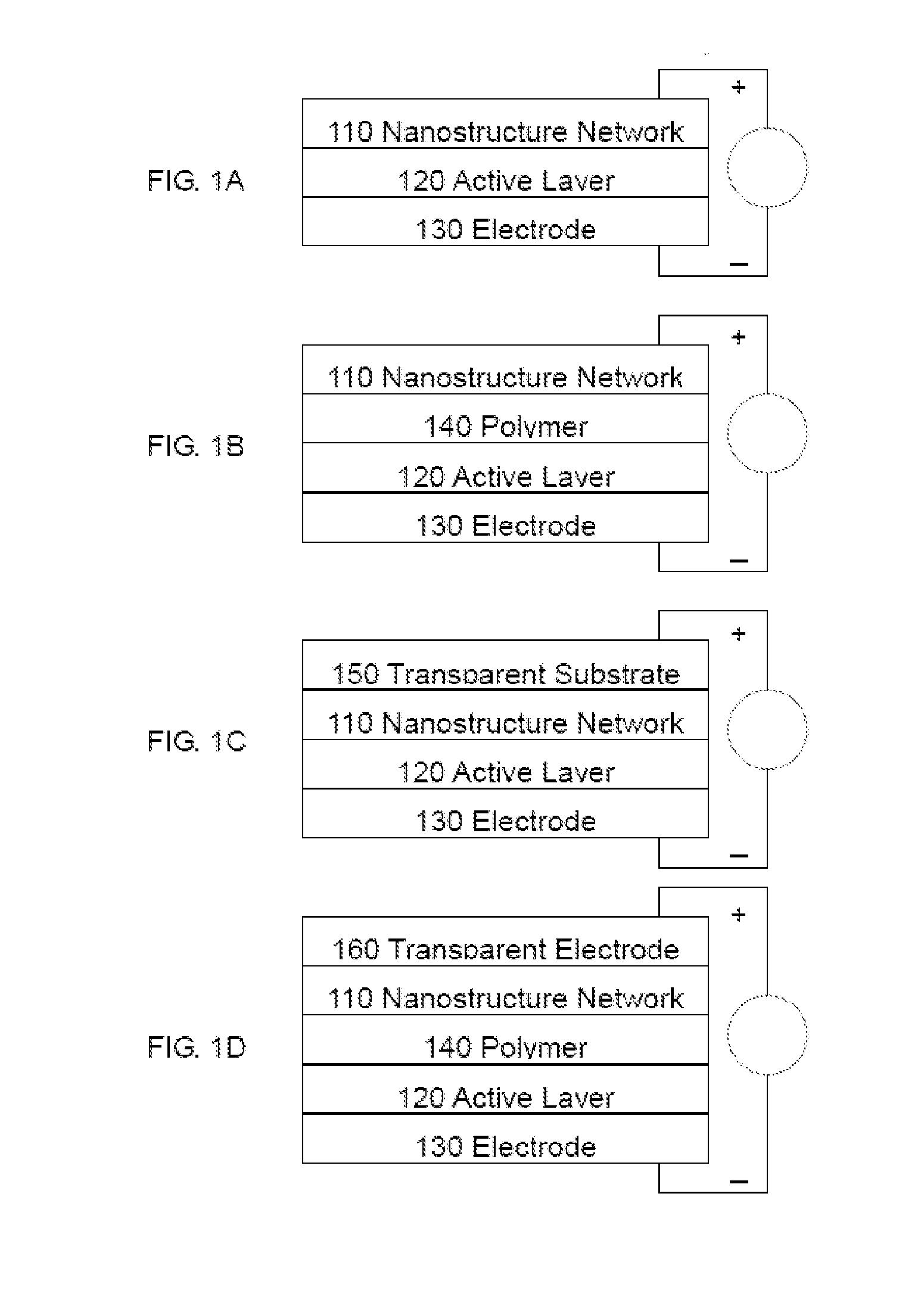
[0029] Referring to FIG. 1A, an optoelectronic device (e.g., solar cell) according to an embodiment of the present invention comprises a nanostructure-film 110, an active layer 120 and an electrode 130. A solar cell is an optoelectronic device that converts photons from the sun (solar light) into electricity—fundamentally, such a device needs to photo-generate charge carriers (e.g., electrons and holes) in an active layer, and separate the charge carriers to conductive electrodes that will transmit the electricity.
[0030] A solar cell active layer 120, according to embodiments of the present invention, is preferably a strong light absorber such as, for example, one based on silicon (e.g., amorphous, protocrystalline, nanocrystalline), cadmium telluride (CdTe), copper indium gallium selenide (CIGS), chalcogenide films of copper indium selenide (CIS), gallium arsenide (GaAs), light absorbing dyes, quantum dots, organic semiconductors (e.g., polymers and small-molecule compounds like p...
PUM
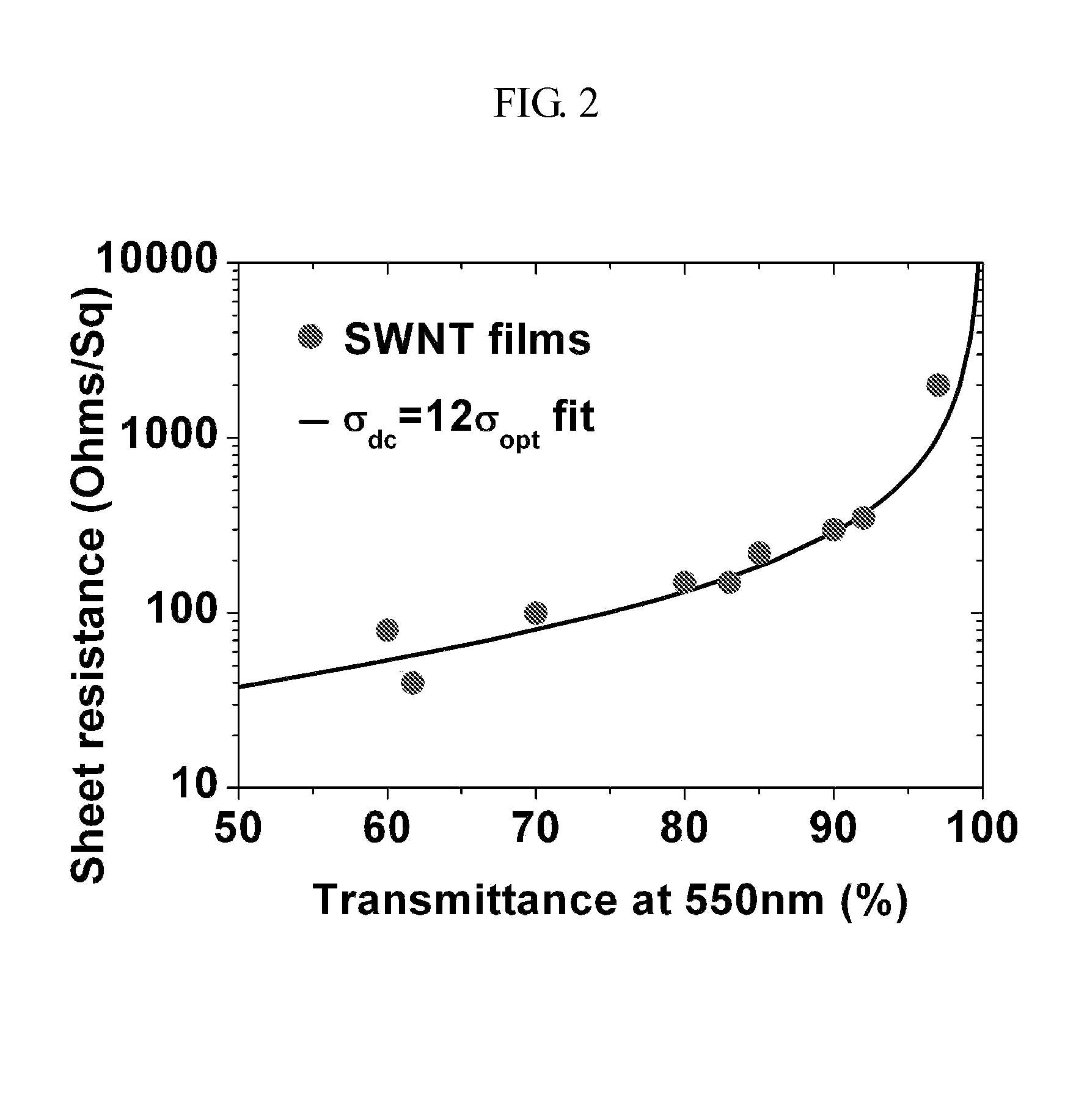
| Property | Measurement | Unit |
|---|---|---|
| Fraction | aaaaa | aaaaa |
| Sheet resistance | aaaaa | aaaaa |
| Electrical conductor | aaaaa | aaaaa |
Abstract
Description
Claims
Application Information