Methods and systems for manufacturing polycrystalline silicon and silicon-germanium solar cells

a technology of polycrystalline silicon and solar cells, applied in the field of methods and systems for producing photovoltaic devices or solar cells, can solve the problems of significant cost increase, plateauing of the reduction of the cost per watt of silicon based solar cells, and exhausted potential of both options, so as to promote widespread acceptance and adoption, and reduce the cost

Inactive Publication Date: 2008-01-31
SENERGEN DEVICES
View PDF25 Cites 36 Cited by
  • Summary
  • Abstract
  • Description
  • Claims
  • Application Information

AI Technical Summary

Benefits of technology

[0007]Of particular advantage, the inventor has discovered a novel method and system for manufacturing polycrystalline silicon and silicon-germanium solar cells or photovoltaic devices that overcomes many of the limitations of the conventional process, and enables production of such devices at significantly reduced cost thereby promoting widespread acceptance and adoption of solar cell technology by the public.

Problems solved by technology

To a great extent, the potential of both of these options has already been exhausted.
As illustrated the cost increases significantly in the final three steps of the process where the single crystal boules are grown, wafers are sawed and then polished.
Moreover, after decades of effort, the reduction in cost per watt of silicon based solar cells is showing signs of having plateaued.
Moreover, the two processes in tandem lead to inherently expensive solar cells and exceeds the key industry metric of “Cost per Watt” thus limiting widespread acceptance and deployment of conventional photovoltaics, as evidenced by an overall movement in the industry towards exploration of materials other than crystalline silicon, such as CIGS, CdTe and amorphous silicon, for achieving cost targets of below $1.00 / watt.
However, these alternative materials do not have the demonstrated field reliability of silicon and the production processes will potentially create a new set of environmental issues.

Method used


Image

  • Methods and systems for manufacturing polycrystalline silicon and silicon-germanium solar cells
  • Methods and systems for manufacturing polycrystalline silicon and silicon-germanium solar cells
  • Methods and systems for manufacturing polycrystalline silicon and silicon-germanium solar cells

Examples


Embodiment Construction

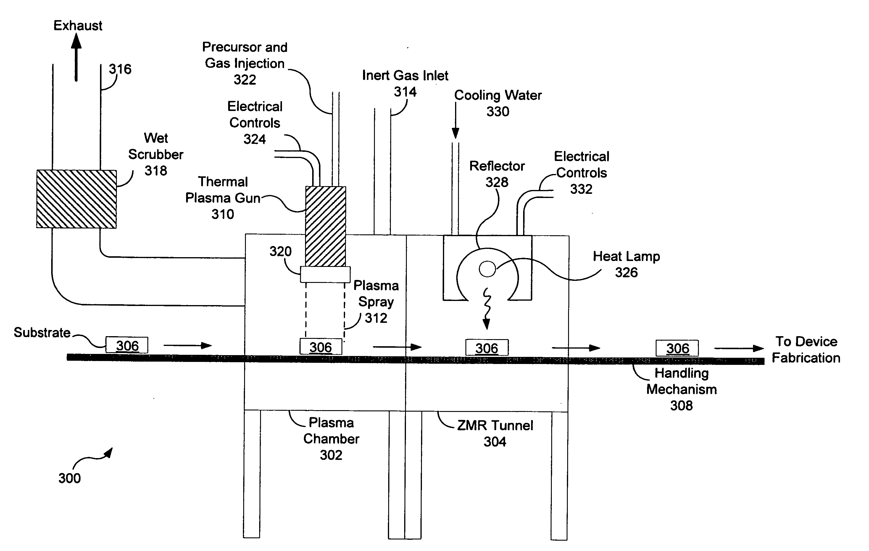
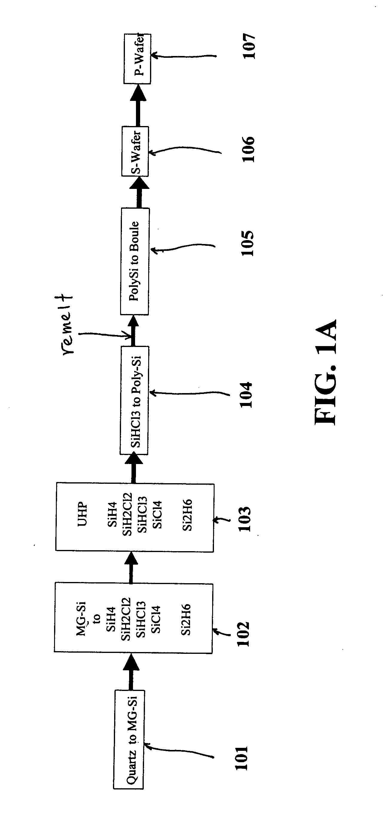
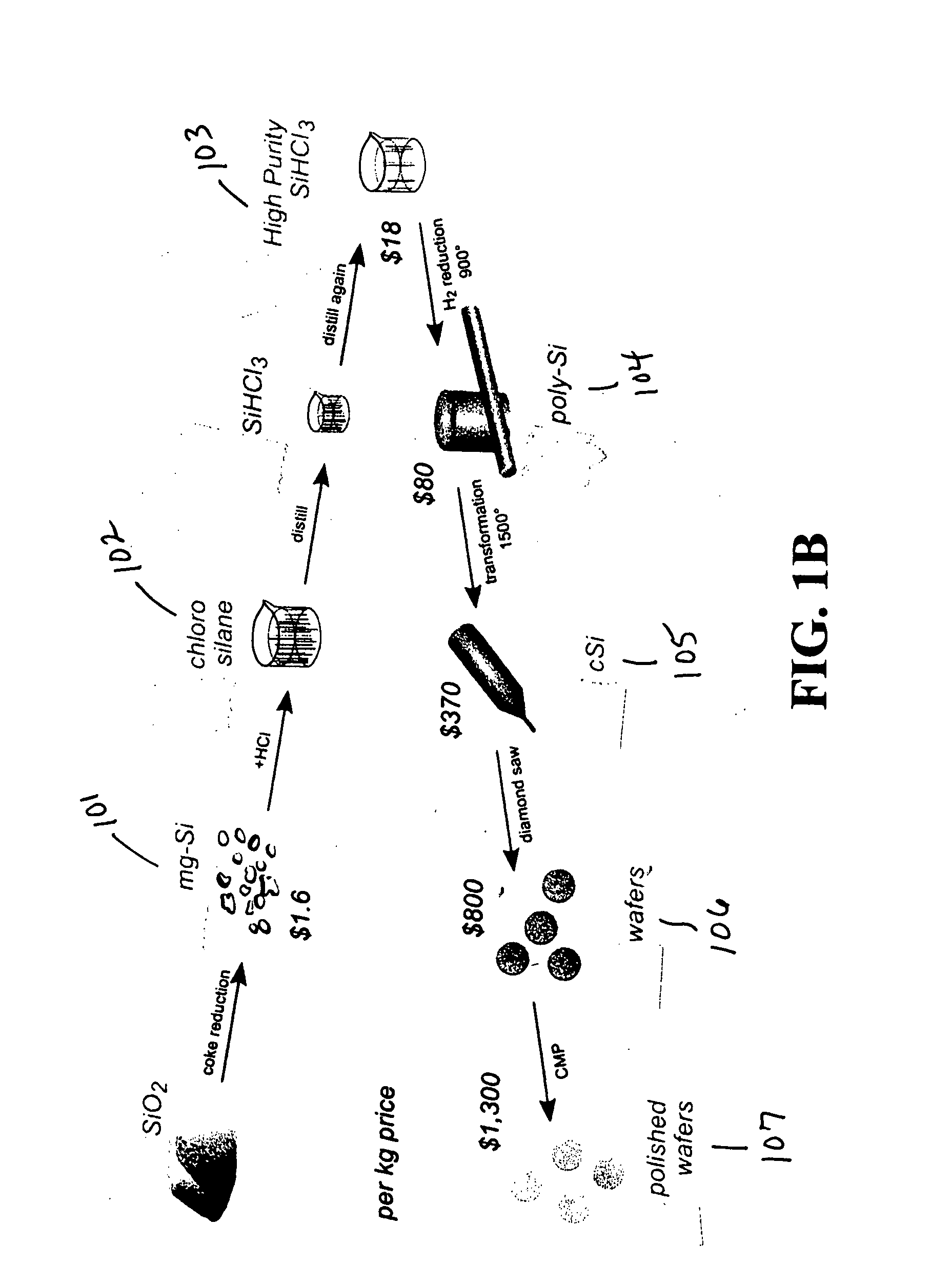
[0022]Embodiments of the present invention are now described in detail. In one embodiment, methods of forming a solar cell or photovoltaic device are provided generally comprising the steps of: generating a plasma stream in a thermal plasma source; injecting one or more silicon intermediate compounds in liquid and / or gaseous form into thermal plasma source wherein the silicon intermediate compounds dissociate; injecting hydrogen into the thermal plasma source; and depositing a polycrystalline silicon film on the surface of one or more substrates located proximate said thermal plasma source, wherein hydrogen is incorporated into the polycrystalline silicon film to promote passivation of silicon grains formed in the polycrystalline silicon film.

[0023]Of particular advantage, liquid and / or gaseous silicon intermediate compounds are employed. In one preferred embodiment, liquid silicon intermediate compounds having a purity of about 99.5% and greater are used. Examples of suitable silic...


PUM

PropertyMeasurementUnit
pressureaaaaaaaaaa
distanceaaaaaaaaaa
distanceaaaaaaaaaa

Abstract

The present invention relates to a novel, unconventional methods and systems for the fabrication of silicon or silicon-germanium photovoltaic cell applications. In some embodiments high purity gaseous and/or liquid intermediate compounds of silicon (or silicon germanium) are converted directly to polycrystalline films by a thermal plasma chemical vapor deposition process or by a thermal plasma spraying technique. The intermediate compounds of silicon (or silicon germanium) are injected into the thermal plasma source where temperatures range from 2000 K to about 20,000 K. The compounds dissociate and silicon (or silicon germanium) is deposited onto substrates. Polycrystalline films having densities approaching the bulk value are obtained on cooling. PN junction photovoltaic cells can be directly prepared by spraying, or doped films after heat treatment are subsequently transformed to viable photovoltaic cells having high efficiency, low cost at a high throughput. In some embodiments a roll-to-roll or a cluster-tool type automated, continuous system is provided.

Description

RELATED APPLICATIONS[0001]This application claims the benefit of, and priority to, U.S. provisional patent application Ser. No. 60 / 833,630 filed on Jul. 28, 2006, the disclosure of which is incorporated by reference herein in its entirety.FIELD OF THE INVENTION[0002]In general, the present invention is directed to methods and systems for producing photovoltaic devices or solar cells. More specifically, the present invention is directed to methods and systems for producing polycrystalline silicon and silicon-germanium solar cells at reduced cost and with high efficiency.BACKGROUND OF THE INVENTION[0003]Electric power generation from silicon photovoltaic devices has gone through significant cost reductions over the years. Widespread adoption, however, will require further breakthroughs in these costs to lower than $1.00 / watt levels. There is a growing belief that these further step function decreases are not likely to come from silicon based cells, as evidenced by a trend towards deve...

Claims


Application Information

Patent Timeline
Patent Type & Authority Applications(United States)
IPC IPC(8): H01L31/18H01L31/00
CPCH01L31/1812Y02E10/546H01L31/182Y02P70/50
Inventor SINHA, SANJAI
Owner SENERGEN DEVICES
Why Eureka
Try Eureka