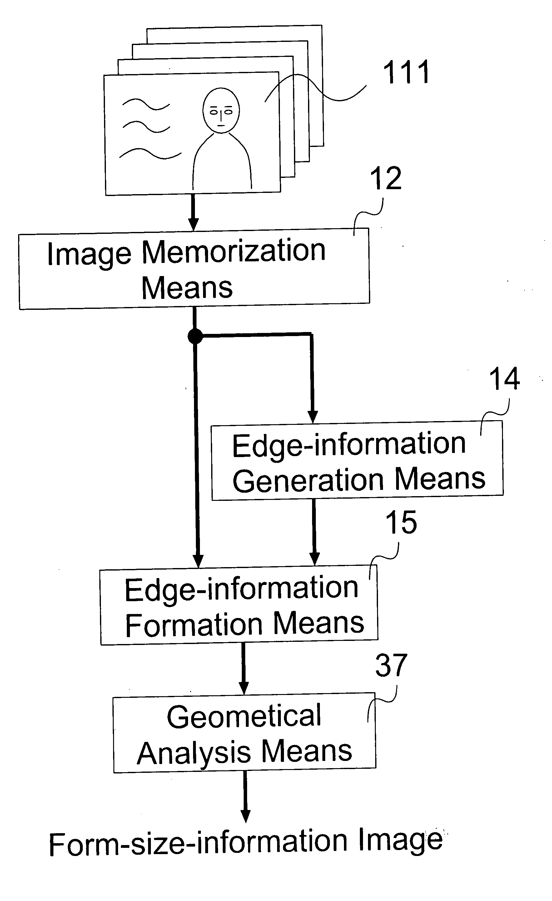
[0632] As suggested by claim 5, the present invention can detect position and size of objects from a formed edge-information image 115, by carrying out
processing every pixel, in parallel. In addition, the present invention can derive form of the objects even though it does not know the size and inclination of the objects beforehand. Since the visual device 2 is also used for preprocessing for recognizing some objects from a frame image of an
animation image taken by a
video camera, or from a still image taken by a
digital camera or captured by a
scanner, the visual device 2 can realize a
pattern recognition device for the
animation image and the still image quickly and cheaply. By outputting 36 or more of transfer-source inclination-redundant information 187, a
system inputting a transfer-source inclination-redundant-information image 188 from the present invention can extract size of objects from the transfer-source inclination-redundant-information image 188, if desired.
[0633] As suggested by claim 6, the present invention can detect position and size of objects from a formed edge-information image 115, by carrying out processing every pixel, in parallel. In addition, the present invention can derive form of the objects even though it does not know the size and inclination of the objects beforehand. Since the visual device 2 is also used for preprocessing for recognizing some objects from a frame image of an
animation image taken by a
video camera, or from a still image taken by a
digital camera or captured by a
scanner, the visual device 2 can realize a
pattern recognition device for the animation image and the still image quickly and cheaply. Since the array operation unit 100 outputs only a detection result, a
system inputting the detection result from the present invention can make its communication mechanism simple.
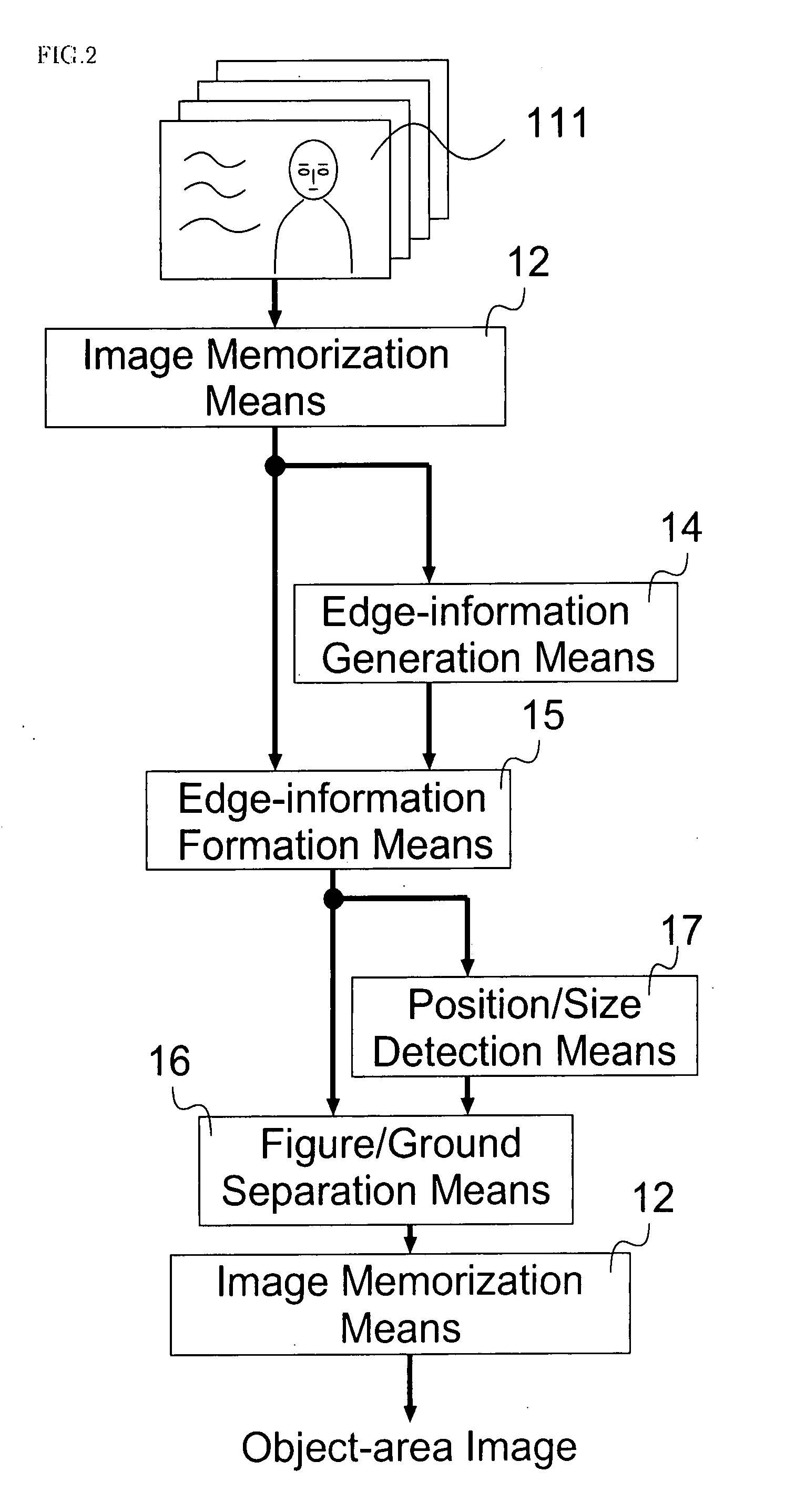
[0634] As suggested by claim 7, the present invention can separate at least one object area 141 segmented by a
binary image from a background area more quickly than separation of the past visual device 2 because each nonlinear oscillator inputs redundant-information 131 as an
external noise. Therefore, a designer of an image sensor 251 can design a fast image sensor 251.
[0635] As suggested by claim 8 and claim 9, the array operation unit 100 transmits calculation data received in only at most two directions. Moreover, many of the calculation data have only to be transmitted in one direction. In short, when the processor 101 writes the calculation datum to the controller 103, a probability that the processor 101 is waited by the controller 103 becomes low. In addition, since the array operation unit 100 can distribute transmission load of the calculation data, the array operation unit 100 can transmit the calculation data efficiently.
[0636] As suggested by claim 10 and claim 11, the
virtual array operation unit 105 transmits calculation data received in only at most two directions. Moreover, many of the calculation data have only to be transmitted in one direction. In short, when the processor 101 writes the calculation datum to the controller 103, a probability that the processor 101 is waited by the controller 103 becomes low. Moreover, the more the number of the array operation units 100 included in the virtual array operation unit 105 becomes, the more times the processor 101 does not write the calculation data to the controller 103. Therefore, the virtual array operation unit 105 can transmit the calculation data efficiently.
[0638] As suggested by claim 13 to claim 16, even though the interlocked counter 401 inputted some
interlocking signals whose phase is different from each other, the interlocked counter 401 selects the latest phase of the signal from the signals, followed by generating its
interlocking signal. Moreover, it can also output the count number synchronized with the phase of the
interlocking signal. Therefore, even though some interlocked counters 401 were distributed in a whole of an LSI (Large Scale
Integrated Circuit), the phases of interlocking signals of all interlocked counters 401 coincide with the latest one if all interlocked counters 401 communicate their interlocking signals with each other. Moreover, the count numbers of the interlocked counters 401 coincide with each other. Since the count numbers become divided signals of the
clock signal, the interlocked counters 401 can supply the same divided signal to a whole of the LSI. On the other hand, since the LSI becomes large and the
clock signal becomes fast, recently, reduction of
power consumption of the LSI is desired. Therefore, an LSI designer must control the clock finely every part of the LSI. However, because of appearance of
propagation delay time caused by long wiring and a problem of
clock skew, it has been difficult for the LSI designer to carry out timing design even though he divided the
clock signal. By using the present invention, then, the LSI designer can design an LSI corresponding to a high-frequency clock signal easily.
[0640] As suggested by claim 18 and claim 19, the higher the resolution of the image sensor 251 becomes, the much less than the number of pixels of the image sensor 251 the number of pixels in a sensor module 252 becomes, by increasing the number of the sensor modules 252. Therefore, a designer of the image sensor 251 can design the sensor module 252 easily. In addition, the manufacturer of the image sensor 251 can make the image sensor 251 in a high yield, in a short time, by arranging only sensor modules 252 already checked on a substrate, using LSI stacking technology. Therefore, an LSI designer can make an image sensor 251, the number of whose pixels is 100 million or more, that is, the number is equal to a human
retina. In addition, an
enforcement form of the image sensor 251 corresponding to the present invention can take out all pixel signals in a shorter time than a time of a general image sensor 251. Moreover, the
enforcement form desires the less number of
signal lines than the number of lines in a pixel-parallel image sensor 251. In the visual device 2, therefore, some virtual array operation units 105 arranged in the shape of a lattice can receive the necessary number of pixel signals in a short time, respectively, by using an
enforcement form of the image sensor 251 corresponding to the present invention.
[0641] As suggested by claim 20, influence of
noise on the image sensor 251 can be reduced because wiring length of
signal lines between a sensor module 252 and the corresponding A / D converter 204 becomes short. In particular, in a case of the invention according to claim 20, total wiring length of signal lines between a sensor module 252 and the corresponding A / D converter 204, and signal lines between a A / D converter 204 and the corresponding digital circuit 402 becomes short. Moreover, they do not cross each other. Therefore, the maximum influence of
noise on the image sensor 251 can be reduced. In addition, the number of A / D
converters 204 is equal to the number of sensor modules 252. Therefore, even though the number of pixels of the image sensor 251 became big, a designer of the image sensor 251 can reduce the number of the A / D
converters 204, by increasing the number of photo-
receptor elements 261 in the sensor module 252. The designer of the image sensor 251, thus, can design a high-resolution image sensor 251, by increasing the number of bits of a
digital signal outputted by the A / D converter 204. In addition, an LSI manufacturer can make an image sensor 251, the number of whose pixels is 100 million or more, which can stimulate human
optic nerve directly, in parallel.

