Monitoring plasma ion implantation systems for fault detection and process control

Inactive Publication Date: 2008-01-31
VARIAN SEMICON EQUIP ASSOC INC +1
View PDF28 Cites 21 Cited by
  • Summary
  • Abstract
  • Description
  • Claims
  • Application Information

AI Technical Summary

Problems solved by technology

Beamline ion implanters are typically designed for efficient operation at relatively high implant energies and may not function efficiently at the low energies required for shallow junction implantation.
This patent does not teach the use of mass analysis for in-situ plasma state measurement or process control

Method used


Image

  • Monitoring plasma ion implantation systems for fault detection and process control
  • Monitoring plasma ion implantation systems for fault detection and process control
  • Monitoring plasma ion implantation systems for fault detection and process control

Examples


first embodiment

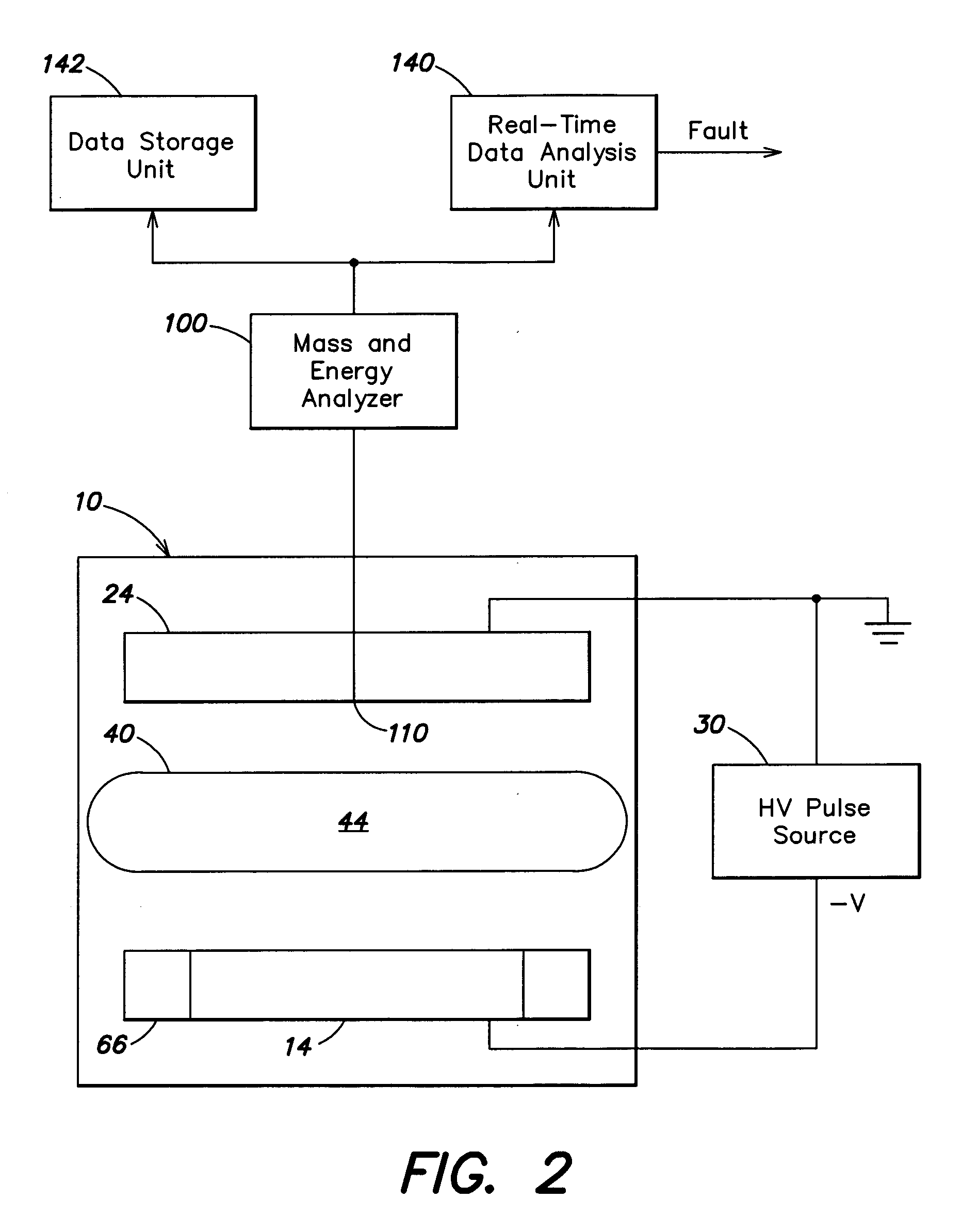
[0032]A simplified schematic block diagram of a plasma ion implantation system in accordance with the invention is shown in FIG. 2. System components shown in FIG. 1 have been omitted for simplicity and to facilitate an understanding of the invention. A mass and energy analyzer 100 is configured to determine the mass and energy of ions associated with plasma 40 in process chamber 10. The mass and energy analyzer 100 extracts ions from process chamber 10 and determines the mass, energy and density of the ions.

[0033]In one example, mass and energy analyzer 100 may be a model EQP mass spectrometer manufactured and sold by Hiden. The EQP mass spectrometer includes an electrostatic sector field energy analyzer followed by a quadrupole mass filter and an ion counting detector. The energy analyzer may include a pair of curved electrodes forming an electrostatic analyzer. The mass analyzer may include a quadrupole mass analyzer. The EQP mass spectrometer operates with a low internal pressur...

second embodiment

[0039]In a second embodiment shown in FIG. 3, an entrance orifice 120 of mass and energy analyzer 100 is located in platen 14. In this embodiment, mass and energy analyzer 100 acquires ions accelerated toward platen 14 by pulse source 30. The embodiment of FIG. 3 requires either that a substrate not be present on platen 14 during mass and energy measurement or requires the use of a special substrate having an opening aligned with entrance orifice 120. The embodiment of FIG. 3 is most useful for maintenance and diagnostic measurements.

third embodiment

[0040]In a third embodiment shown in FIG. 4, an entrance orifice 130 of mass and energy analyzer 100 is located in guard ring 66 adjacent to a substrate support surface of platen 14. In this embodiment, ion mass and energy can be analyzed during plasma ion implantation of wafer 20. Mass and energy analyzer 100 acquires ions accelerated from plasma 40 toward platen 14. The configuration of FIG. 4 permits real-time, in-situ mass and energy measurement during plasma ion implantation. It will be understood that two or more entrance orifices may be located around the periphery of platen 14. The entrance orifices may have a common connection to mass and energy analyzer 100 or may be successively connected to mass and energy analyzer 100. In other embodiments, two or more entrance orifices may be associated with respective mass and energy analyzers.

[0041]FIG. 4 further illustrates mass and energy analyzer 100 utilized in a closed loop configuration for process control. The measurements acq...


PUM

PropertyMeasurementUnit
Timeaaaaaaaaaa
Massaaaaaaaaaa
Speedaaaaaaaaaa

Abstract

A plasma ion implantation system includes a process chamber, a source for producing a plasma in the process chamber, a platen for holding a substrate in the process chamber and a pulse source for generating implant pulses for accelerating ions from the plasma into the substrate. In one aspect, the system includes a plasma monitor configured to measure ion mass and energy in the process chamber and an analyzer configured to determine an operating condition of the system in response to the measured mass and energy. In another aspect, the system includes a data acquisition unit configured to acquire samples of the implant pulses and analyzer configured to determine an operating condition of the system based on the acquired samples.

Description

FIELD OF THE INVENTION[0001]This invention relates to systems and methods for plasma ion implantation of substrates and, more particularly, to methods and apparatus for monitoring operation of plasma ion implantation systems.BACKGROUND OF THE INVENTION[0002]Ion implantation is a standard technique for introducing conductivity-altering impurities into semiconductor wafers. In a conventional beamline ion implantation system, a desired impurity material is ionized in an ion source, the ions are accelerated to form an ion beam of prescribed energy, and the ion beam is directed at the surface of the wafer. Energetic ions in the beam penetrate into the bulk of the semiconductor material and are embedded into the crystalline lattice of the semiconductor material to form a region of desired conductivity.[0003]A well-known trend in the semiconductor industry is toward smaller, higher speed devices. In particular, both the lateral dimensions and the depths of features in semiconductor devices...

Claims


Application Information

Patent Timeline
IPC IPC(8): C23C16/52B05C11/00H01J37/32
CPCH01J37/32412H01J37/30H01J37/32H01L21/265
Inventor FANG, ZIWEIKO, SUNG-CHEONWINDER, EDMUND J.DISTASO, DANIELGODET, LUDOVICKOO, BON WOONGSCHEUER, JAY T.
Owner VARIAN SEMICON EQUIP ASSOC INC
Why Eureka
Try Eureka