
In-situ process diagnostics of in-film aluminum during plasma deposition

a technology of in-situ process and aluminum, applied in the direction of plasma technique, instruments, coatings, etc., can solve the problems of metal contaminants, particularly detrimental to dielectric layers, contaminants that can be deposited on surfaces, etc., and achieve the effect of less cos

Inactive Publication Date: 2008-02-07
APPLIED MATERIALS INC
View PDF10 Cites 16 Cited by
  • Summary
  • Abstract
  • Description
  • Claims
  • Application Information

AI Technical Summary

Benefits of technology

[0007]Systems and methods in accordance with various embodiments of the present invention provide for in-process determination of contaminant levels. Such determination can be relatively instantaneous, and can be much less expensive than traditional contaminant measurement techniques.
[0009]A maximum amount threshold can be set for any of the measured contaminants, such that when the determined amount of contaminant concentration in the plasma approaches, is at or near, or exceeds the threshold, processing of substrates in the processing chamber can be stopped. After processing is stopped, the chamber can be cleaned to remove any contamination and can be treated or otherwise processed to reduce the amount of contaminant in the plasma resulting from the process chamber. Treating the process chamber can include any process known in the art, such as seasoning chamber components by applying a layer of material such as silicon oxide on the components to prevent particles such as aluminum particles from passing from the components into the plasma during processing.

Problems solved by technology

A problem with existing processes for manufacturing devices such as semiconductor chips is that certain contaminants can be deposited onto the surfaces and into films of these devices during manufacture.
Metal contaminants such as aluminum can be particularly detrimental to dielectric layers in these devices as the metal contaminants will exhibit electrical properties after thermal processing that can negatively affect gate oxides and other device components and functionality.
A common metal contaminant deposited in such processes is aluminum.
Further, the measurement process can take a substantial amount of time, such as about 3-5 days when shipped to an outside lab, which can result in the production of a number of wafers with unacceptable aluminum content.

Method used


Image

  • In-situ process diagnostics of in-film aluminum during plasma deposition
  • In-situ process diagnostics of in-film aluminum during plasma deposition
  • In-situ process diagnostics of in-film aluminum during plasma deposition

Examples


Embodiment Construction

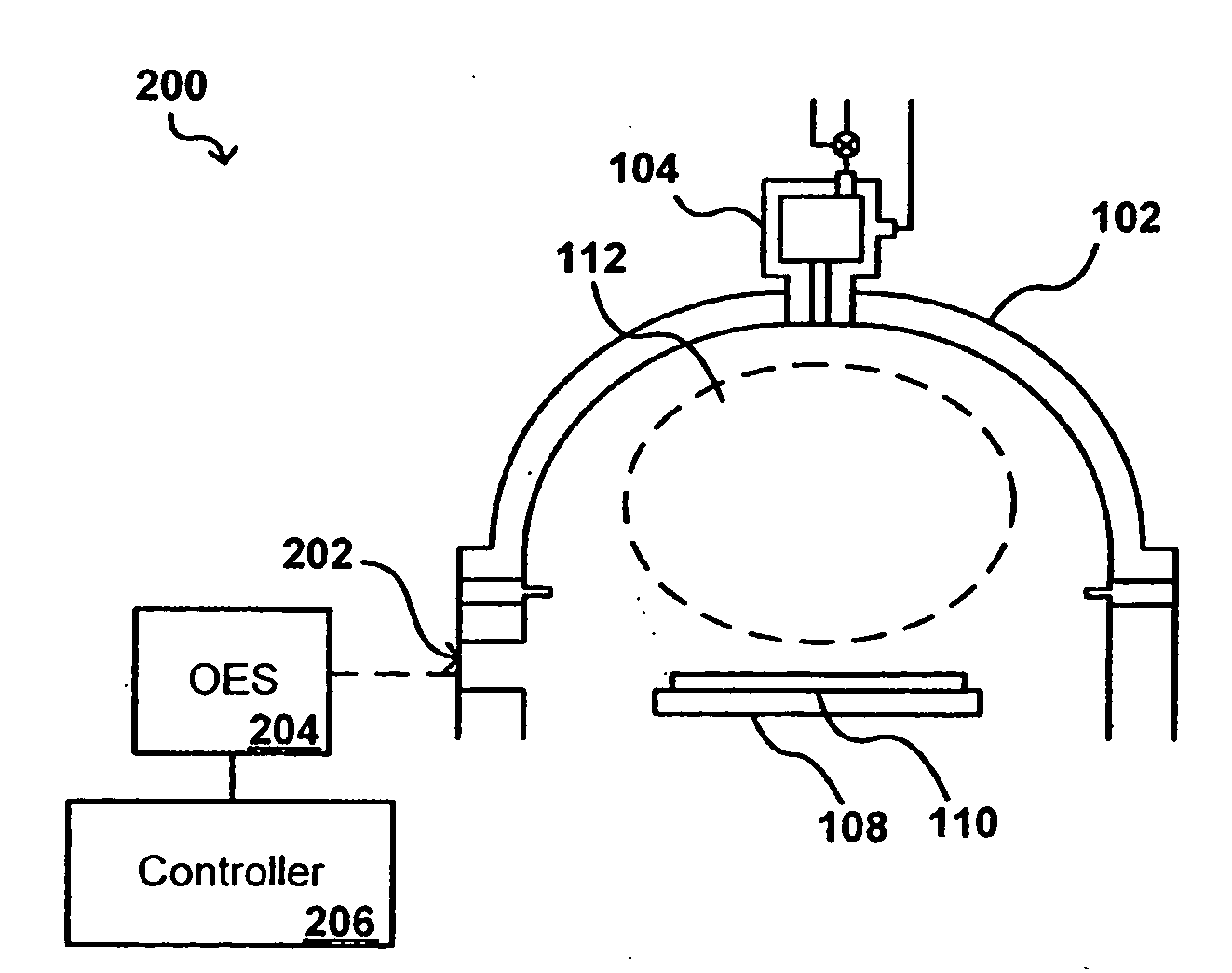
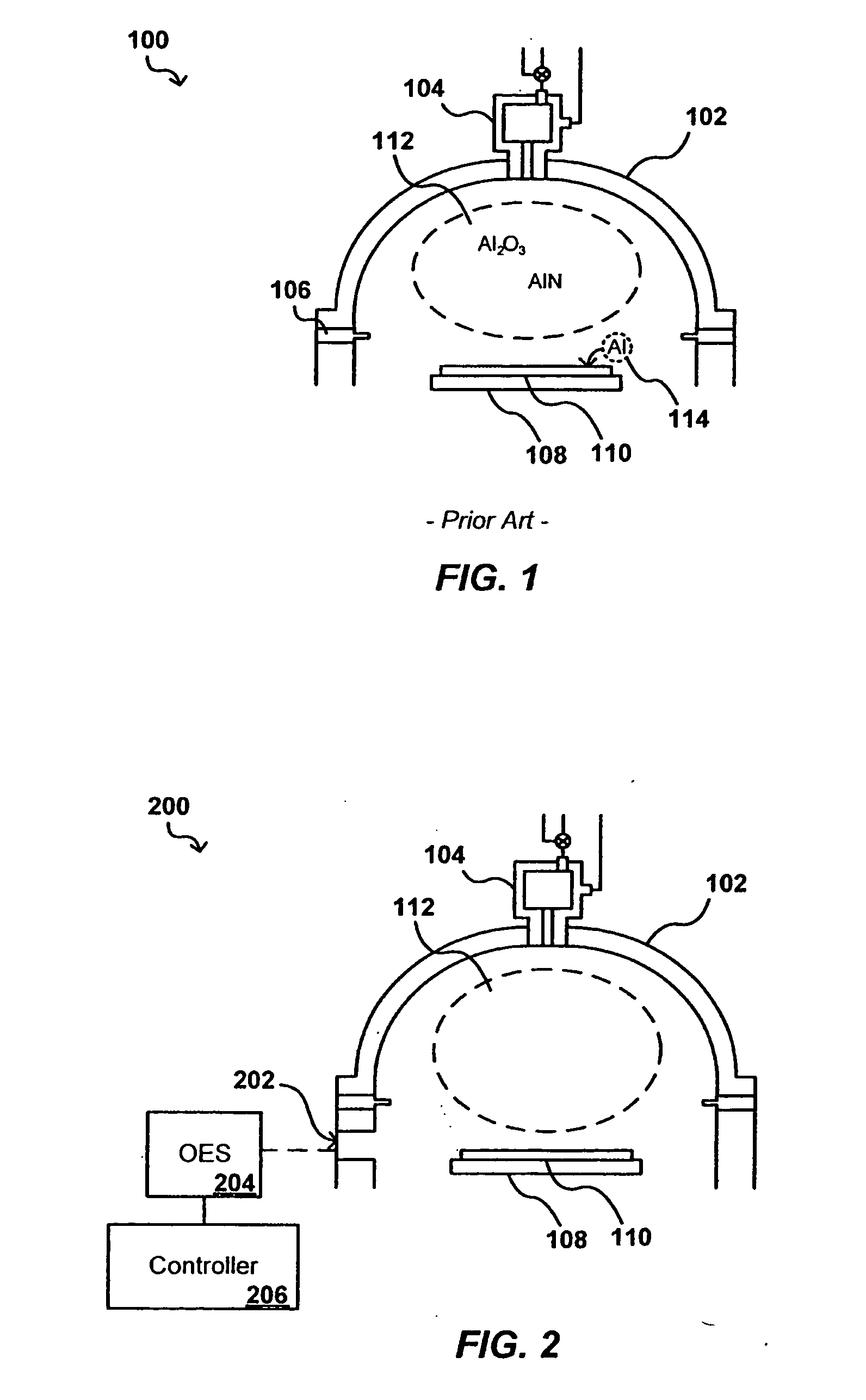
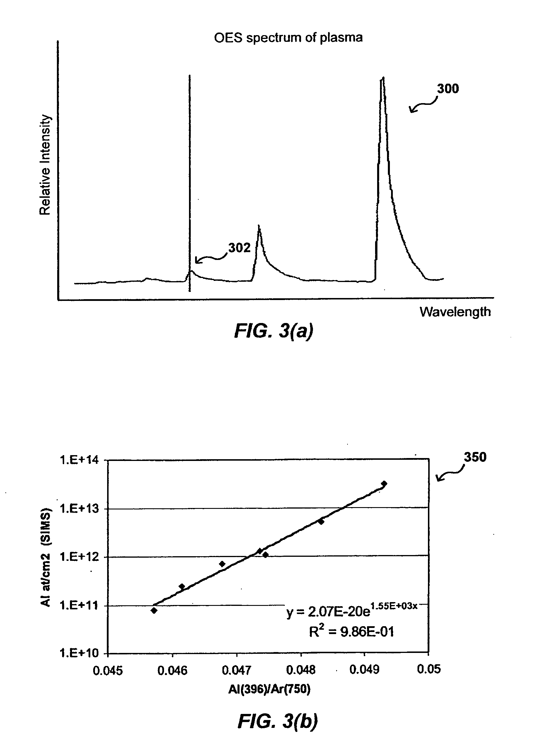
[0018]Systems and methods in accordance with various embodiments of the present invention can overcome the aforementioned and other deficiencies in existing processing systems by providing for an in-situ determination of contaminant content. In one embodiment, the optical emission of a plasma in a chemical vapor deposition (CVD) process is examined during a deposition in order to determine the aluminum content of the plasma. A maximum aluminum content threshold can be used to determine when the plasma is at or near a maximum aluminum content, such that processing can be stopped and the CVD system can be treated to reduce the amount of aluminum contaminants passing into the plasma and, accordingly, into or onto the processed devices.

[0019]For example, FIG. 1 illustrates a cross-section of a portion of an exemplary plasma deposition chamber 100 useful for depositing a film on a substrate 110, such as a silicon wafer. The substrate is placed on a substrate support 108 in the chamber, w...


PUM

PropertyMeasurementUnit
temperatureaaaaaaaaaa
pressuresaaaaaaaaaa

Abstract

The concentration of various contaminants in a plasma can be monitored during processing of a substrate such as a silicon wafer, in order to prevent an unacceptable amount of contamination from being deposited on the substrate. The radiation emitted from the plasma through a window in the processing chamber during processing can be detected and measured by a tool such as an optical emission spectrograph (OES) and the relative intensity of peaks in the spectrum corresponding to various contaminants can be analyzed in order to determine contaminant concentration. In one embodiment, the concentration of aluminum in a plasma is monitored during a plasma chemical vapor deposition (CVD) process in order to ensure that the amount of aluminum in the produced device is lower than a maximum threshold amount.

Description

BACKGROUND OF THE INVENTION[0001]The present invention relates to the deposition of material on a substrate. More particularly, the invention relates to a method and apparatus for monitoring the aluminum content of a plasma when an integrated circuit is manufactured using a plasma processing technique.[0002]One of the steps in the fabrication of modern semiconductor devices is the formation of a thin film on a semiconductor substrate through a chemical reaction of selected gases. One such deposition process is referred to as chemical vapor deposition (“CVD”). Conventional thermal CVD processes supply reactive gases to the surface of a substrate, where heat-induced chemical reactions take place to produce a desired film. Plasma-enhanced CVD techniques, on the other hand, promote excitation and / or dissociation of the reactant gases through the application of radio-frequency (“RF”), microwave, or other energy to a reaction zone near the substrate surface, thereby creating a plasma. The...

Claims


Application Information

Patent Timeline
Patent Type & Authority Applications(United States)
IPC IPC(8): C23F1/00G06F19/00H01L21/306H05H1/24C23C16/00
CPCC23C16/4401H01J37/32972H01J37/32935C23C16/52
Inventor PARK, SOONAMAHMAD, FARHANMUNGEKAR, HEMANT P.LEE, YOUNG S.
Owner APPLIED MATERIALS INC
Learn More