Semiconductor memory device comprising a plurality of static memory cells

a memory device and static technology, applied in static storage, information storage, digital storage, etc., can solve the problems of difficult to compensate for the change of threshold voltage, complicated structure achieving the two kinds of power supplies, and become difficult to perform semiconductor memory devices. achieve the effect of simple circuit structure and stable writing and reading of data

Active Publication Date: 2008-02-14
RENESAS ELECTRONICS CORP
View PDF7 Cites 53 Cited by
  • Summary
  • Abstract
  • Description
  • Claims
  • Application Information

AI Technical Summary

Benefits of technology

[0018]An object of the invention is to provide a semiconductor memory device that has a simple circuit structure, and allows stable writing and reading of data even with a lower power supply voltage.
[0019]Another object of the invention is to provide a semiconductor memory device that adjusts the selected word line potential in a manner flexibly following variations in threshold voltage of the memory cell transistor, and thereby can ensure write and read margins even with a low power supply voltage.
[0020]Still another object of the invention is to provide a semiconductor memory device that sets a word line potential to an optimum value depending on variations in threshold voltage of the memory cell transistor independently of an operation temperature, and thereby can ensure write and read margins.
[0022]In this semiconductor memory device according to the invention, the resistance element which is the passive element and the pull-down element set the voltage on the power supply node of the word line driver. Therefore, the potential of selected word line can be low in the read operation, and a conductance of an access transistor in the memory cell can be reduced so that a static memory margin in the read operation can be improved.
[0023]The device simply uses the resistance element which is the passive element and the pull-down circuit, and does not require the power supply for the level changing so that a power supply structure can be simple. Since the resistance element which is the passive element is used, a resistance value of the resistance element slightly increases when its temperature increases, but the resistance element has temperature characteristics that have an extremely low sensitivity to the temperature. Therefore, the potential change of the word line with respect to the temperature change is very small, and the pull-down circuit can be configured to follow only the changes in threshold voltage of the memory cell transistor. More specifically, the pull-down element is formed of a transistor similar to the memory cell transistor. Thereby, the voltage level of the word line can be adjusted according to the variations in threshold voltage of the memory cell transistor. When the pull-down element is formed of an N-channel MOS transistor, and particularly is at a low temperature, a threshold voltage Vth is high, but a mobility is also high so that a value of a current flowing through the N-channel MOS transistor for the pull-down does not change to a large extent. Conversely, when the temperature is high, threshold voltage Vth of the N-channel MOS transistor lowers, and the mobility also lowers so that the current hardly changes similarly to the above. Accordingly, the temperature dependence of the potential of selected word line can be eliminated, and the potential of selected word line can be set to an optimum value depending on the threshold voltage of the memory cell in a wide temperature range.

Problems solved by technology

Consequently, it becomes difficult in a semiconductor memory device to perform stable writing and reading of data with a low power supply voltage.
Therefore, two kinds of voltages are required as the memory cell power supply voltage, which results in a problem that a structure achieving the two kinds of power supplies becomes complicated.
Therefore, even when a threshold voltage of the memory cell transistor varies due to variations in process parameter, the voltage level does not change according to such variations, and it is difficult to compensate for the changes in threshold voltage.
Therefore, it is difficult to ensure reliably the write and read margins when changes or the like occur in electric characteristics such as a threshold voltage of the memory cell transistor.

Method used


Image

  • Semiconductor memory device comprising a plurality of static memory cells
  • Semiconductor memory device comprising a plurality of static memory cells
  • Semiconductor memory device comprising a plurality of static memory cells

Examples


first embodiment

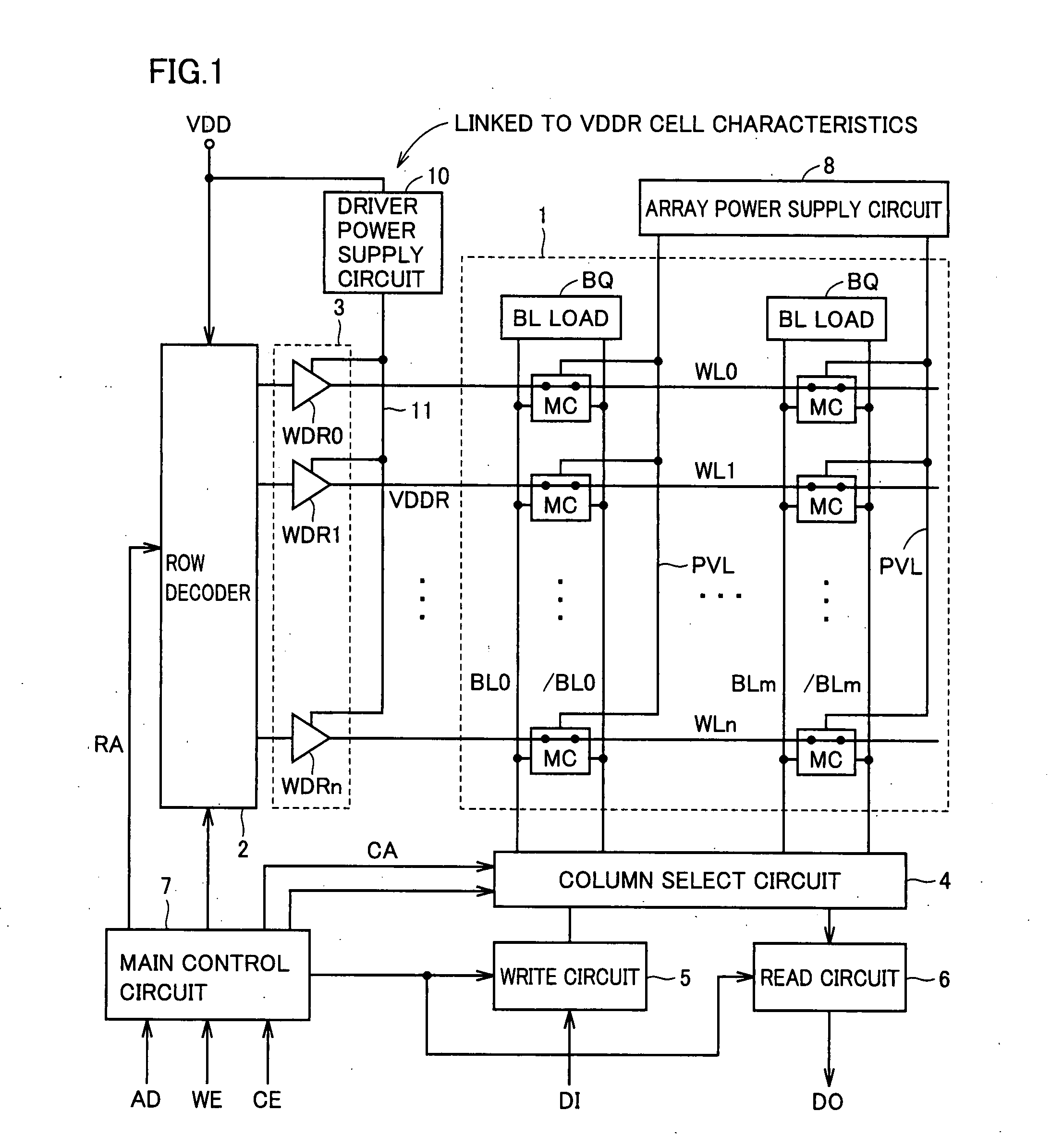
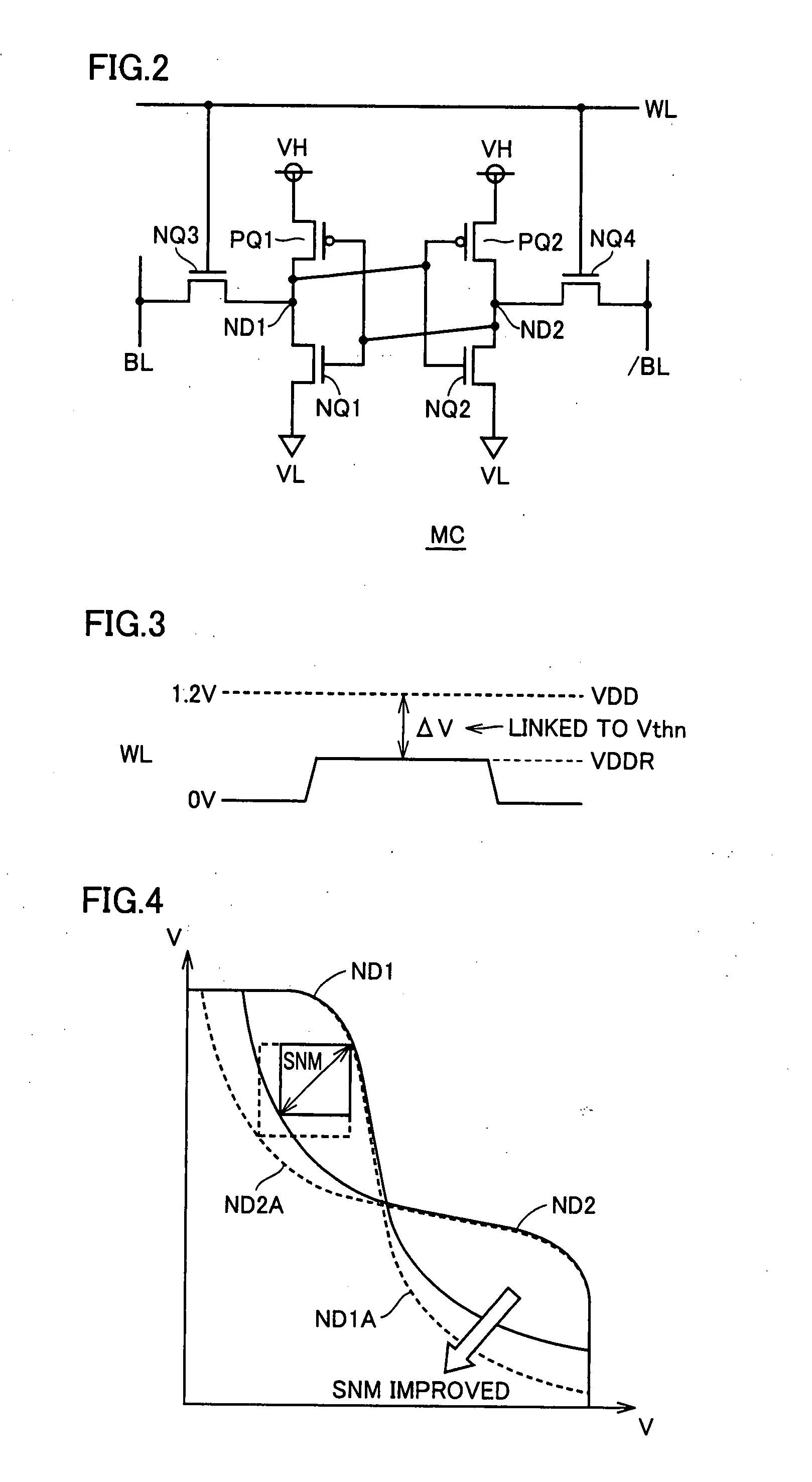
[0083]FIG. 5 schematically shows a major structure of the semiconductor memory device according to a first embodiment of the invention. In an example of memory cell array 1 shown in FIG. 5, memory cells MC are arranged in four rows and one column, and word lines WL0-WL3 are arranged corresponding to the respective rows. Word line drive circuit 3 includes word line drivers WDR0-WDR3 corresponding to word lines WL0-WL3, respectively. Driver power supply circuit 10 is provided with a series connection of a resistance element 20 and a pull-down element 21 shared among word line drivers WDR0-WDR3. For example, resistance element 20 employs an N+ polycrystalline silicon interconnection. Preferably, this resistance element is a non-silicide N+ polycrystalline silicon interconnection. Resistance element 20 that employs a passive element instead of a transistor can offer an advantage that a resistance value thereof does not change to a large extent even when a temperature changes. Pull-down ...

second embodiment

[0105]FIG. 9 shows a structure of driver power supply circuit 10 according to a second embodiment of the invention. In FIG. 9, driver power supply circuit 10 includes resistance element 20 connected between the power supply node and driver power supply line 11, and pull-down transistor 21 connected between driver power supply line 11 and a ground node. Resistance element 20 and pull-down transistor 21 have the same structures as those in the first embodiment. Therefore, pull-down transistor 21 is formed of the unit transistors (UTRs) of K in number connected in parallel.

[0106]Driver power supply circuit 10 further includes an N-channel MOS transistor 22 that is connected between the power supply node and an internal node 25, and has a gate connected to the power supply node, and an N-channel MOS transistor 24 that is connected between internal node 25 and the ground node, and has a gate connected to internal node 25. These transistors 21, 22 and 24 form a pull-down circuit that lowe...

third embodiment

[0124]FIG. 12 schematically shows a structure of driver power supply circuit 10 according to a third embodiment of the invention. FIG. 12 likewise shows word line drivers WDR0-WDR3 in word line drive circuit 3, also shows memory cells MC arranged in four rows and one column in memory cell array 1 and word lines WL0-WL3 corresponding to the respective rows.

[0125]Driver power supply circuit 10 in FIG. 12 differs from driver power supply circuit 10 shown in FIG. 9 in the following structure. A resistance element 26 is used in stead of N-channel MOS transistor 24 formed of the logic transistor. Similarly to resistance element 20, resistance element 26 has an interconnection width equal to the gate length (channel length) of the N-channel MOS transistor in memory cell MC (see FIG. 8). Other structures of driver power supply circuit 10 shown in FIG. 12 are the same as those of the driver power supply circuit shown in FIG. 9. The corresponding portions bear the same reference numbers, and ...


PUM


Abstract

A driver power supply circuit stepping down a power supply voltage is arranged at a power supply node of a word line driver. The driver power supply circuit includes a non-silicide resistance element of N+ doped polycrystalline silicon, and a pull-down circuit lowering a voltage level of the driver power supply node. The pull-down circuit includes a pull-down transistor having the same threshold voltage characteristics as a memory cell transistor pulling down a voltage level of the driver power supply node, and a gate control circuit adjusting at least a gate voltage of the pull-down transistor. The gate control circuit corrects the gate potential of the pull-down transistor in a manner linked to variations in threshold voltage of the memory cell transistor.

Description

BACKGROUND OF THE INVENTION[0001]1. Field of the Invention[0002]The present invention relates to a semiconductor memory device, and particularly to a structure of a static semiconductor memory device that allows stable writing and reading of data even under operation conditions of a low voltage.[0003]2. Description of the Background Art[0004]When transistor elements are miniaturized according to the progression of miniaturization technologies, voltage scaling depending on the miniaturization is required in view of reliability of the elements and power consumption. As the miniaturization is performed, an influence of variations in manufacturing parameter increases, and causes large variations in threshold voltage of transistors (i.e., insulated gate field-effect transistors to be referred to as “MOS transistors” hereinafter) that form a memory cell. Consequently, it becomes difficult in a semiconductor memory device to perform stable writing and reading of data with a low power suppl...

Claims


Application Information

Patent Timeline
Patent Type & Authority Applications(United States)
IPC IPC(8): G11C8/08
CPCG11C5/147G11C11/413G11C11/412G11C8/08G11C11/41
Inventor YABUUCHI, MAKOTONII, KOJI
Owner RENESAS ELECTRONICS CORP
Why Eureka
Try Eureka