Method for manufacturing semiconductor device

a manufacturing method and semiconductor technology, applied in the field of manufacturing semiconductor devices, can solve the problems of film formation for a long time, the epitaxial layer of the n type on the n+ type substrate needs to be thickened, and the manufacturing time and manufacturing cost are reduced, and the width of the first conductive type semiconductor region and the width of the second conductive type semiconductor film is reduced. , the effect of reducing the on-state resistance of the devi

Active Publication Date: 2008-02-14
DENSO CORP
View PDF5 Cites 53 Cited by
  • Summary
  • Abstract
  • Description
  • Claims
  • Application Information

AI Technical Summary

Benefits of technology

[0021]In the above method, a manufacturing time and a manufacturing cost are reduced, and the impurity concentration in the second conductive type semiconductor film is sufficiently controlled to be a predetermined value. Further, the substrate provides the periphery layer as a terminal end of the device.
[0022]According to a sixth aspect of the present disclosure, a method for manufacturing a semiconductor device includes: forming a plurality of trenches on a first side of a semiconductor substrate, wherein the substrate has a first conductive type; forming a first conductive type semiconductor region on an inner wall of each trench by an epitaxial growth method, wherein an impurity concentration of the first conductive type semiconductor region is higher than an impurity concentration of the substrate, and wherein the substrate between adjacent two trenches and the first conductive type semiconductor region in the adjacent two trenches provide a first column; forming a second conductive type semiconductor film on the first conductive type semiconductor region in each trench so that the second conductive type semiconductor film in each trench provides a second column, wherein the first and second columns are alternately repeated along with a predetermined direction in parallel to the first side of the substrate; thinning a second side of the substrate, the second side being opposite to the first side; and increasing an impurity concentration of a thinned second side of the substrate so that a first conductive type layer is provided, wherein the impurity concentration of the first conductive type layer is higher than an impurity concentration of the first conductive type semiconductor region. A part of the substrate disposed on a periphery of the substrate provides a periphery layer, and the first column provides a drift layer so that a vertical type first-conductive-type channel transistor is formed. In the above method, the first conductive type semiconductor region is formed on the inner wall of each trench by the epitaxial growth method, and the second conductive type semiconductor film is formed on the first conductive type semiconductor region in each trench. Thus, the width of the first conductive type semiconductor region and the width of the second conductive type semiconductor film are reduced, respectively. Thus, the on-state resistance of the device is reduced. Further, a manufacturing time and a manufacturing cost are reduced, and the impurity concentration in the second conductive type semiconductor film is sufficiently controlled to be a predetermined value. Further, the substrate provides the periphery layer as a terminal end of the device.

Problems solved by technology

However, when it is intended to realize the lower ON-resistance and the higher withstand voltage, it has been revealed by the inventors that problems to be stated below are posed.
As the first problem, for the purpose of manufacturing a device portion of high withstand voltage, the epitaxial layer of the N type on the N+ type substrate needs to be thickened.
By way of example, the thickness of the N type epitaxial layer needs to be at least 30 μm for a withstand voltage of 600 V, and it needs to be at least 60 μm for a withstand voltage of 1200 V. In order to obtain such a large thickness, film formation for a long time is required, and a process cost becomes high.
Besides, as the second problem, when both the high withstand voltage and the low ON-resistance are to be attained, the widths dn and dp of the respective epitaxial layers of the N type and P type need to be made small so as to heighten the concentrations of the respective layers, and the respective layers need to be thickened.
However, when the trench is narrowed in order to make small the width of, for example, the P type epitaxial layer, the P type epitaxial layer formed earlier at the opening part of the trench closes up this opening part of the trench, to incur the problem that the P type epitaxial layer is not formed at the bottom of the trench.
However, a long time is expended on film formation, and a process cost becomes high.

Method used


Image

  • Method for manufacturing semiconductor device
  • Method for manufacturing semiconductor device
  • Method for manufacturing semiconductor device

Examples


first embodiment

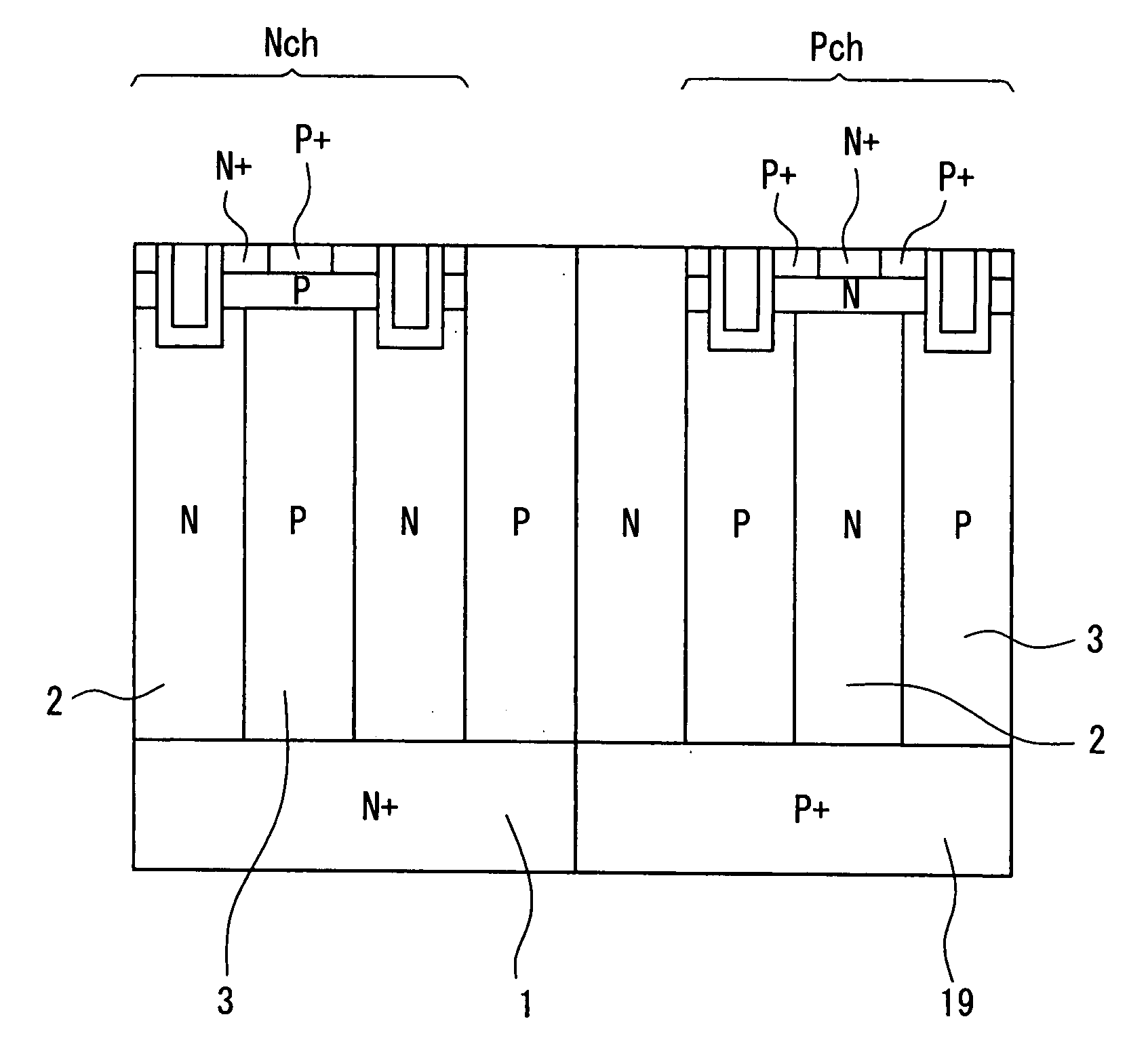
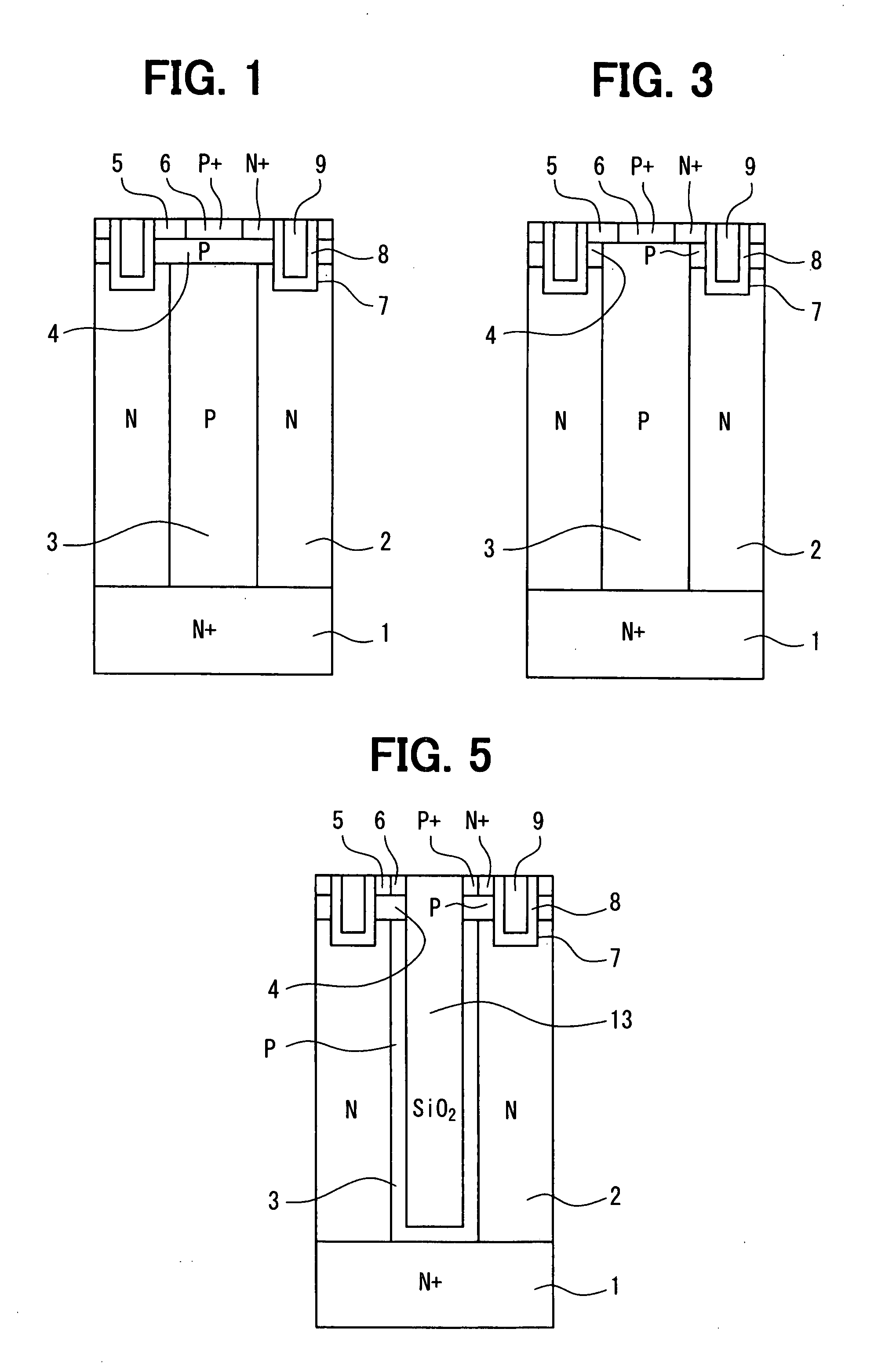
[0039]FIG. 1 is a schematic sectional view of a semiconductor device according to the first embodiment. As shown in FIG. 1, the semiconductor device is formed with a large number of MOS transistors of N-channel type. An N type layer 2 (corresponding to a first layer of first conductivity type) and a P type layer 3 (corresponding to a first layer of second conductivity type) are formed on an N+ type layer 1 (corresponding to a second layer of the first conductivity type) as drift regions, and a super-junction structure in which the N type layer 2 and P type layer 3 are alternately arranged in the planar direction of the N+ type layer 1 is formed.

[0040]Besides, a P type channel layer 4 is formed at the front surface layer parts of the N type layer 2 and the P type layer 3. Further, an N+ type source layer 5 is formed on a side opposing to the N type layer 2, within the front surface layer part of the P type channel layer 4, and a P+ type layer 6 is formed on a side opposing to the P t...

second embodiment

[0058]In this embodiment, only parts different from the parts of the first embodiment will be described. This embodiment features that, after a device portion has been formed on an N type substrate 10, a super-junction structure is formed.

[0059]FIG. 3 is a schematic sectional view of a semiconductor device according to this embodiment. In this embodiment, any P type channel layer 4 is not existent in a P type layer 3, unlike in the semiconductor device shown in FIG. 1 in the first embodiment. More specifically, a P type channel layer 4 is formed at the front surface layer part of an N type layer 2, and an N+ type source layer 5 is formed at the front surface layer part of the P type channel layer 4. In addition, a trench 7 reaching the N type layer 2 is formed penetrating through the N+ type source layer 5 and the P type channel layer 4. A gate insulating film 8 and a gate layer 9 are successively formed on the inner wall surface of the trench 7, whereby a trench gate structure is c...

third embodiment

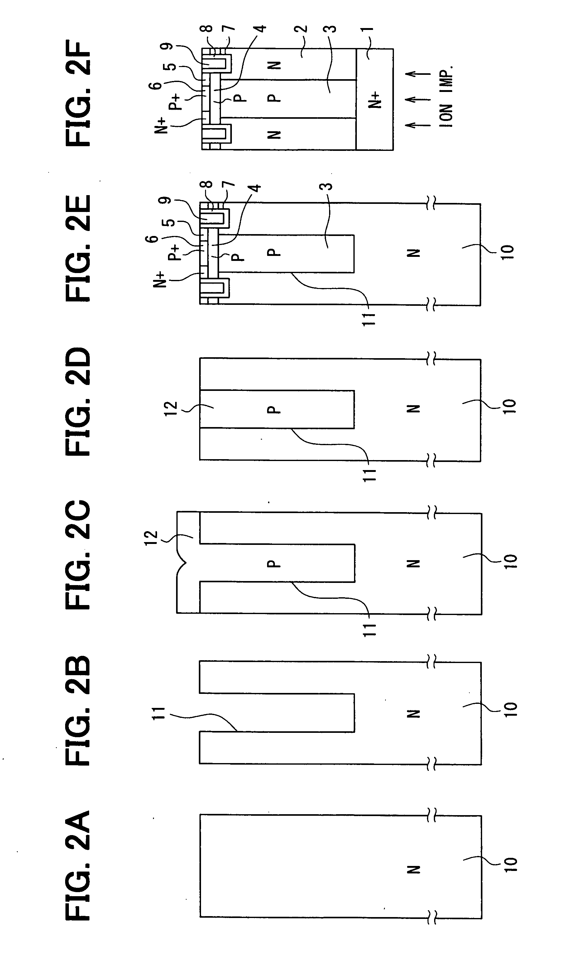
[0067]In this embodiment, only parts different from the parts of the foregoing embodiments will be described. This embodiment features that a P type layer 3 is not buried completely within a trench 11, but that in a state where a P type epitaxial layer 12 is formed on the wall surface of the trench 11, an insulating layer is buried into the P type epitaxial layer 12 conforming to the shape of the trench 11, thereby to configure a repeated structure which consists of an N type layer 2 and the P type layer 3 formed of the P type epitaxial layer 12.

[0068]FIG. 5 is a schematic sectional view of a semiconductor device according to this embodiment. As shown in the figure, in this embodiment, an oxide film 13 and the P type layer 3 are successively formed on the inner wall surface of the trench 11 which is provided in each N type layer 2 formed with a trench gate structure. An SiO2 film, for example, is adopted as the oxide film 13.

[0069]Next, a method for manufacturing the semiconductor d...


PUM


Abstract

A manufacturing method of a semiconductor device includes: forming multiple trenches on a semiconductor substrate; forming a second conductive type semiconductor film in each trench to provide a first column with the substrate between two trenches and a second column with the second conductive type semiconductor film in the trench, the first and second columns alternately repeated along with a predetermined direction; thinning a second side of the substrate; and increasing an impurity concentration in a thinned second side so that a first conductive type layer is provided. The impurity concentration of the first conductive type layer is higher than the first column. The first column provides a drift layer so that a vertical type first-conductive-type channel transistor is formed.

Description

CROSS REFERENCE TO RELATED APPLICATION[0001]This application is based on Japanese Patent Application No. 2006-219477 filed on Aug. 11, 2006, the disclosure of which is incorporated herein by reference.FIELD OF THE INVENTION[0002]The present invention relates to a method for manufacturing a semiconductor device.BACKGROUND OF THE INVENTION[0003]Heretofore, there has been known a semiconductor device in which a super-junction structure is adopted for, for example, a power MOS transistor of vertical type. The “superjunction structure” is a configuration in which N type layers and P type layers to serve as a drift region are alternately arranged in the planar direction of a substrate. Owing to the adoption of such a structure, an electric field from a source toward a drain is also directed from the N type layers to the P type layers. Accordingly, the electric field can be prevented from concentrating in one place between the source and the drain, and in turn, the prevention of insulation...

Claims


Application Information

Patent Timeline
Patent Type & Authority Applications(United States)
IPC IPC(8): H01L21/336H01L21/66
CPCH01L21/823814H01L21/823885H01L29/0634H01L29/0649H01L29/7813H01L29/1095H01L29/66734H01L29/7803H01L29/7811H01L29/0653Y10S438/977
Inventor YAMAGUCHI, HITOSHIMIYAJIMA, TAKESHI
Owner DENSO CORP
Why Eureka
Try Eureka