
Circuit board structure and method for fabricating the same

Inactive Publication Date: 2008-02-21
PHOENIX PRECISION TECH CORP
View PDF3 Cites 51 Cited by
  • Summary
  • Abstract
  • Description
  • Claims
  • Application Information

AI Technical Summary

Benefits of technology

[0010] In view of the above drawbacks of the prior art, a primary objective of the present invention is to provide a circuit board structure and a method for fabricating the same, so as to increase the bonding strength between a circuit layer and a dielectric layer.
[0012] A further objective of the present invention is to provide a circuit board structure and a method for fabricating the same, so as to effectively control the shape of circuits and enhance the electrical performance of the circuit board.
[0018] The circuit board structure and the method for fabricating the same according to the present invention can enhance the bonding strength between dielectric layers and circuit layers, thereby improving product reliability and quality.
[0019] Moreover, in the circuit board structure and the method for fabricating the same according to the present invention, a fine circuit process is not limited by the resolution of the resist layer and the bonding strength between the resist layer and the dielectric layer, such that fine circuit can be formed as desired for use with miniaturized and high-performance electronic products and the thickness of circuits and lines can be effectively controlled.

Problems solved by technology

However, when fabricating fine circuits by the semi-additive process or the pattern plating method for the multi-layer substrate, due to the small line space of the fine circuits, the bonding strength between the circuit layers and the dielectric layers is not strong enough such that product reliability and quality are compromised.
On the other hand, if enhancing the bonding strength between the circuit layers and the dielectric layers, the line width would be undesirably increased, which is not favorable for fabrication of the fine circuits.
However, because of the constraints on the exposure and development processes, precision of the laser drilling and the bonding strength of the conductive layer, for example, due to the limits of ultraviolet wavelength, diffraction during exposure makes peripheral portions of photoresist patterns blurred, such that it is not easy to define the line width, reduce the line width and control the line thickness.

Method used


Image

  • Circuit board structure and method for fabricating the same
  • Circuit board structure and method for fabricating the same
  • Circuit board structure and method for fabricating the same

Examples


Embodiment Construction

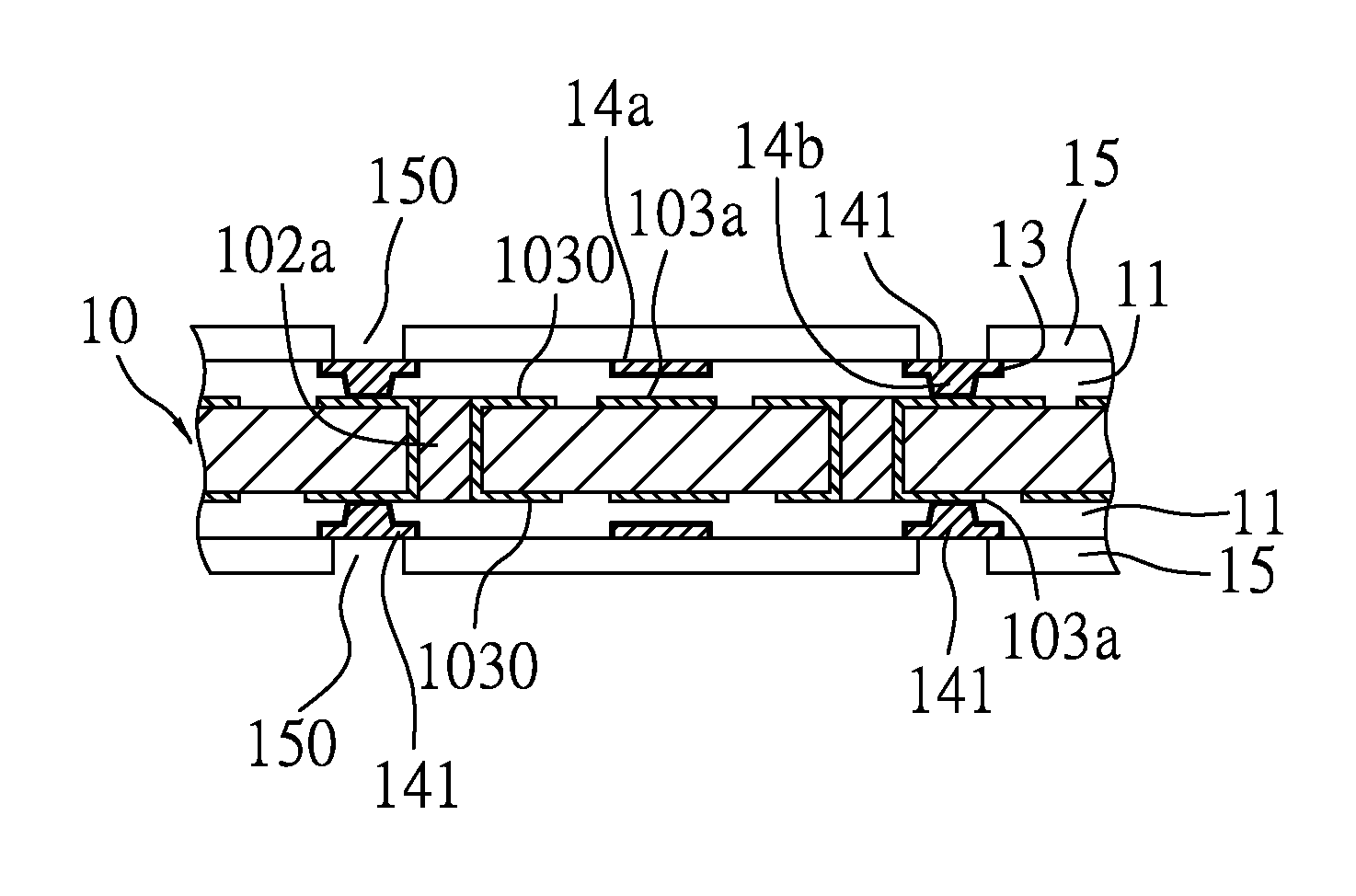
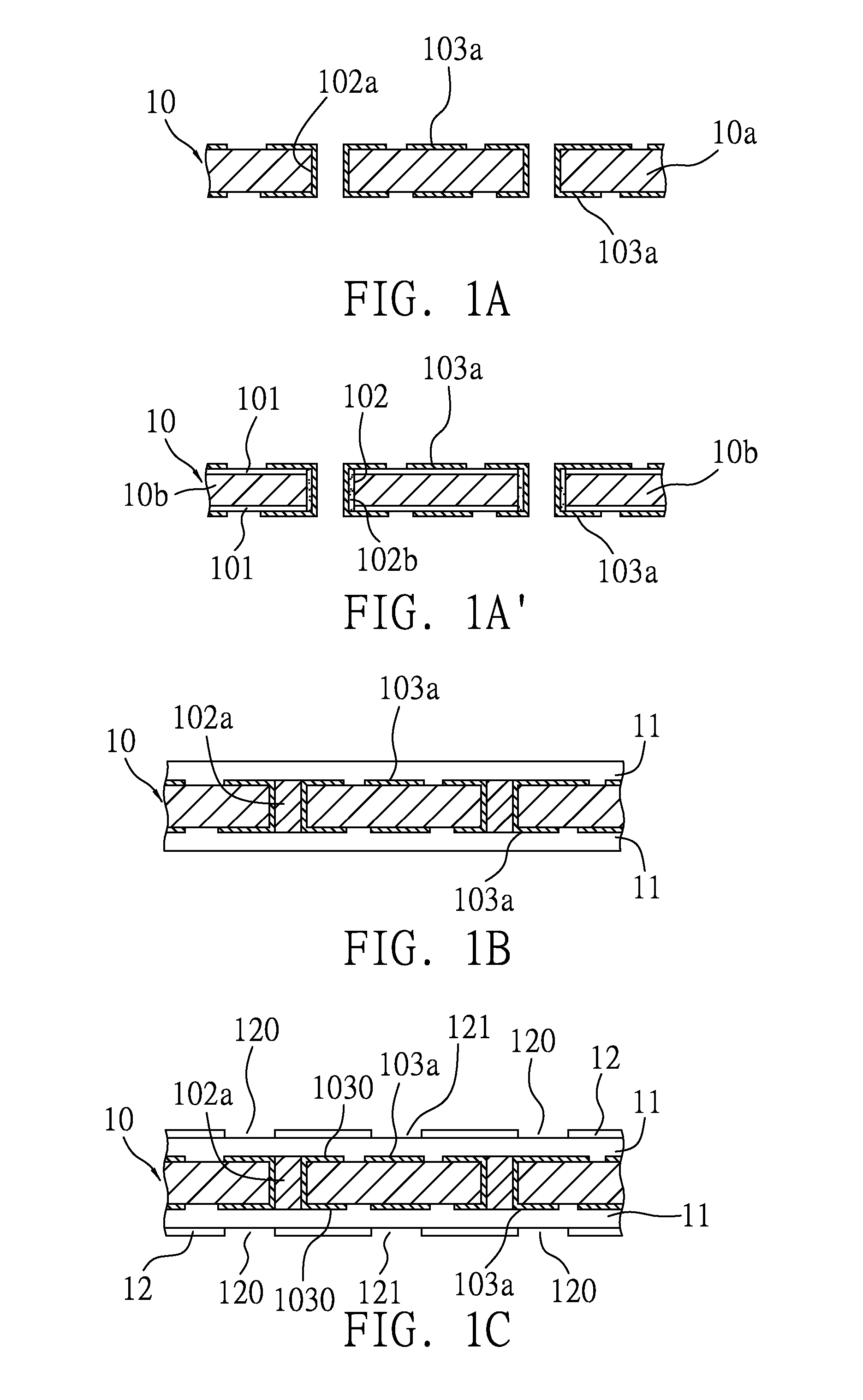
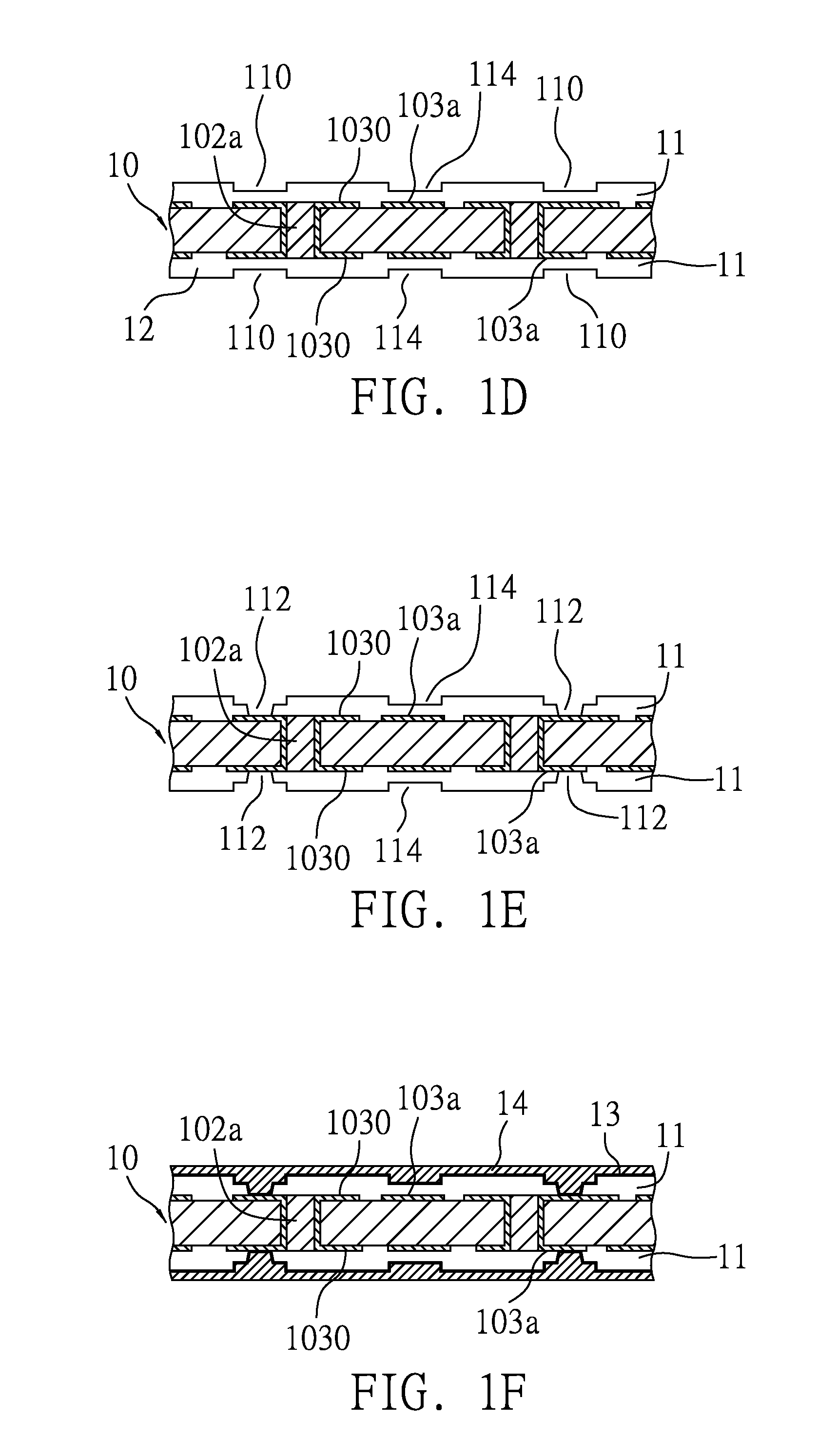
[0025] Preferred embodiments of a circuit board structure and a method for fabricating the same as proposed in the present invention are described as follows with reference to FIGS. 1A to 1H, 2A to 2G, 3A to 3G and 4A to 4C. It should be understood that the drawings are simplified schematic diagrams only showing the elements relevant to the present invention, and the layout of elements could be more complicated in practical implementation.

[0026]FIGS. 1A to 1H are cross-sectional views showing a circuit board structure and a method for fabricating the same in accordance with a first preferred embodiment of the present invention.

[0027] Referring to FIGS. 1A and 1A′, at least one core board 10, 10′ is provided. The core board 10, 10′ can be a single-layer or multi-layer circuit board formed with a first circuit layer on at least one surface thereof. For example, as shown in FIG. 1A, the circuit board comprises a ceramic board 10a as a core thereof, wherein the ceramic board 10a is fo...


PUM


Abstract

A circuit board structure and a method for fabricating the same are proposed. A substrate with a first circuit layer formed on at least one surface thereof is provided. A dielectric layer is formed on the surface of the substrate, and a plurality of first and second openings are formed in the dielectric layer, wherein the second openings expose electrical connection pads of the first circuit layer. A metal layer is formed on the surface of the dielectric layer and in the first and second openings. By removing the metal layer on the surface of the dielectric layer, a second circuit layer is formed in the second openings, and a conductive structure is formed in the second openings for electrical connection with the first circuit layer. The present invention improves the bonding strength between the circuit layer and the dielectric layer, and the ability of fabricating fine circuits.

Description

CROSS-REFERENCE TO RELATED APPLICATIONS [0001] Under 35 USC 119(e), this application claims foreign priority to Taiwan application No. 095105026, filed Feb. 15, 2006, all of which is incorporated herein by reference. FIELD OF THE INVENTION [0002] The present invention relates to circuit board structures and methods for fabricating the same, and more particularly, to a build-up circuit board with fine circuits and a method for fabricating the build-up circuit board. BACKGROUND OF THE INVENTION [0003] In response to the booming electronics industry, electronic products have been developed with multi-functionality and high performance. Further with a view to fabricating highly integrated and miniaturized semiconductor packages and carrying more active components and circuits, a substrate serving as a carrier in a semiconductor package has been made in the form from a double-layer circuit board to a multi-layer circuit board. The multi-layer circuit board employs an interlayer connectio...

Claims


Application Information

Patent Timeline
IPC IPC(8): H05K1/11H01R12/04
CPCH05K3/0032H05K3/0035H05K3/0041H05K3/045H05K2201/0166H05K3/4602H05K3/465H05K3/4661H05K3/107H05K3/42
Inventor HSU, SHIH-PINGYEN, YA-LUN
Owner PHOENIX PRECISION TECH CORP
Learn More