Light-Emitting Device

a light-emitting device and light-emitting technology, applied in semiconductor devices, lasers, laser details, etc., to achieve the effect of improving light extraction efficiency and low light extraction efficiency

Inactive Publication Date: 2008-02-21
IND TECH RES INST
View PDF5 Cites 25 Cited by
  • Summary
  • Abstract
  • Description
  • Claims
  • Application Information

AI Technical Summary

Benefits of technology

[0009]Compared with the prior art, the light-emitting device of the present invention arranges the transparent electrode and the photonic crystals to improve the light extraction efficiency. The transparent electrode of the light-emitting device diffuses the cur

Problems solved by technology

Low output efficiency of light-emitting devices such as light-emitting diode (LED) originates mainly from low light extraction efficiency, which means

Method used


Image

  • Light-Emitting Device
  • Light-Emitting Device
  • Light-Emitting Device

Examples


Embodiment Construction

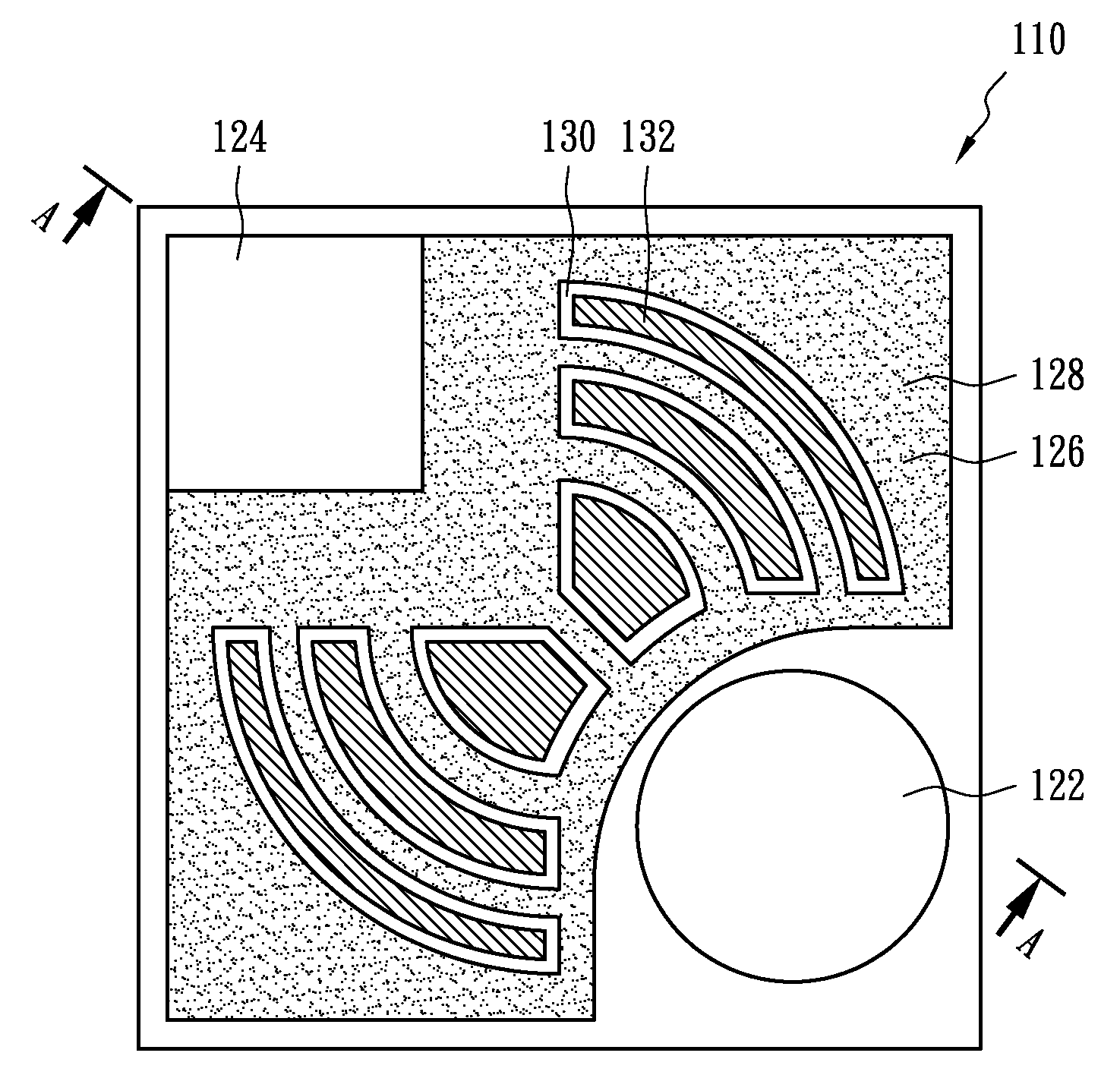
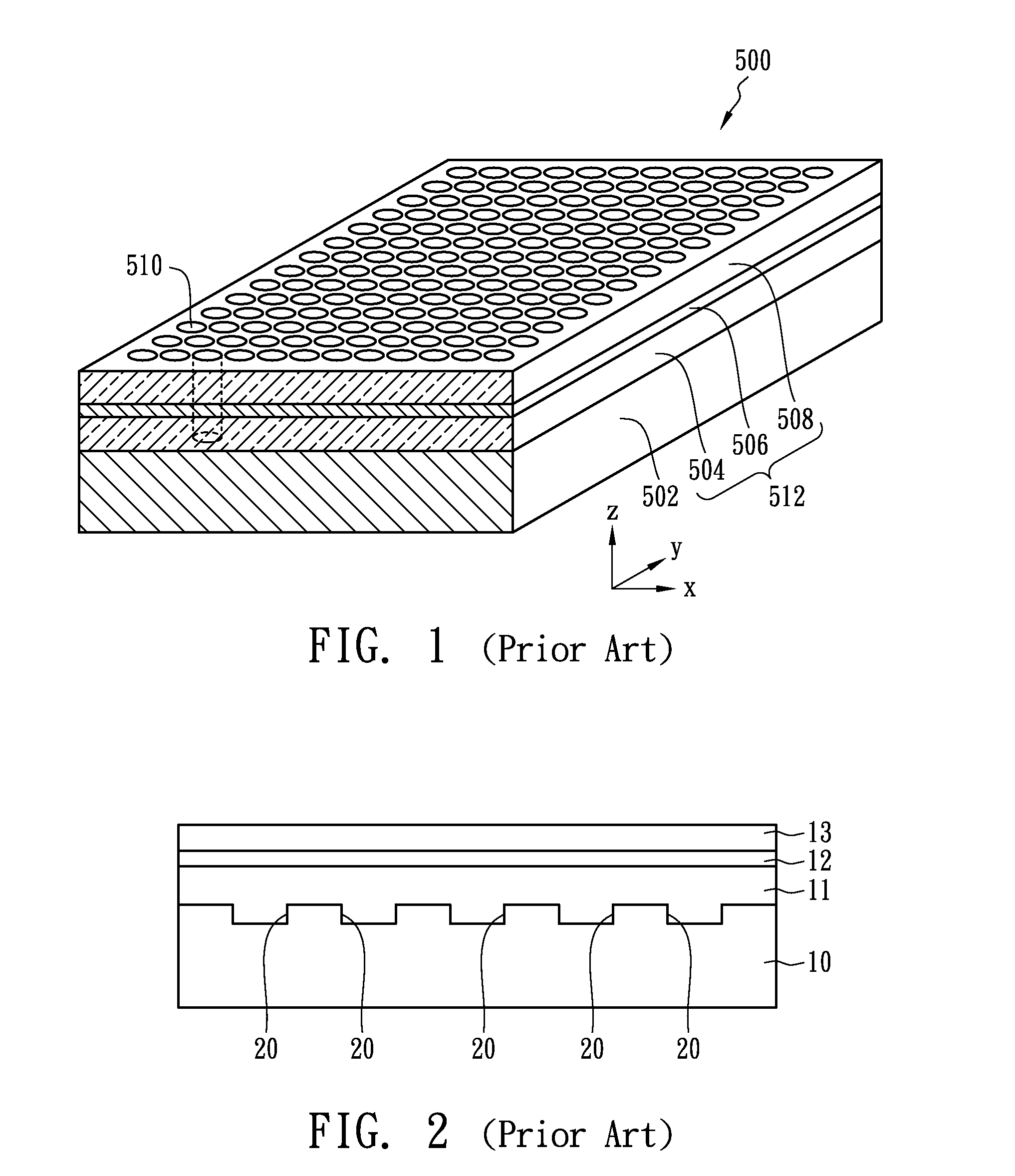
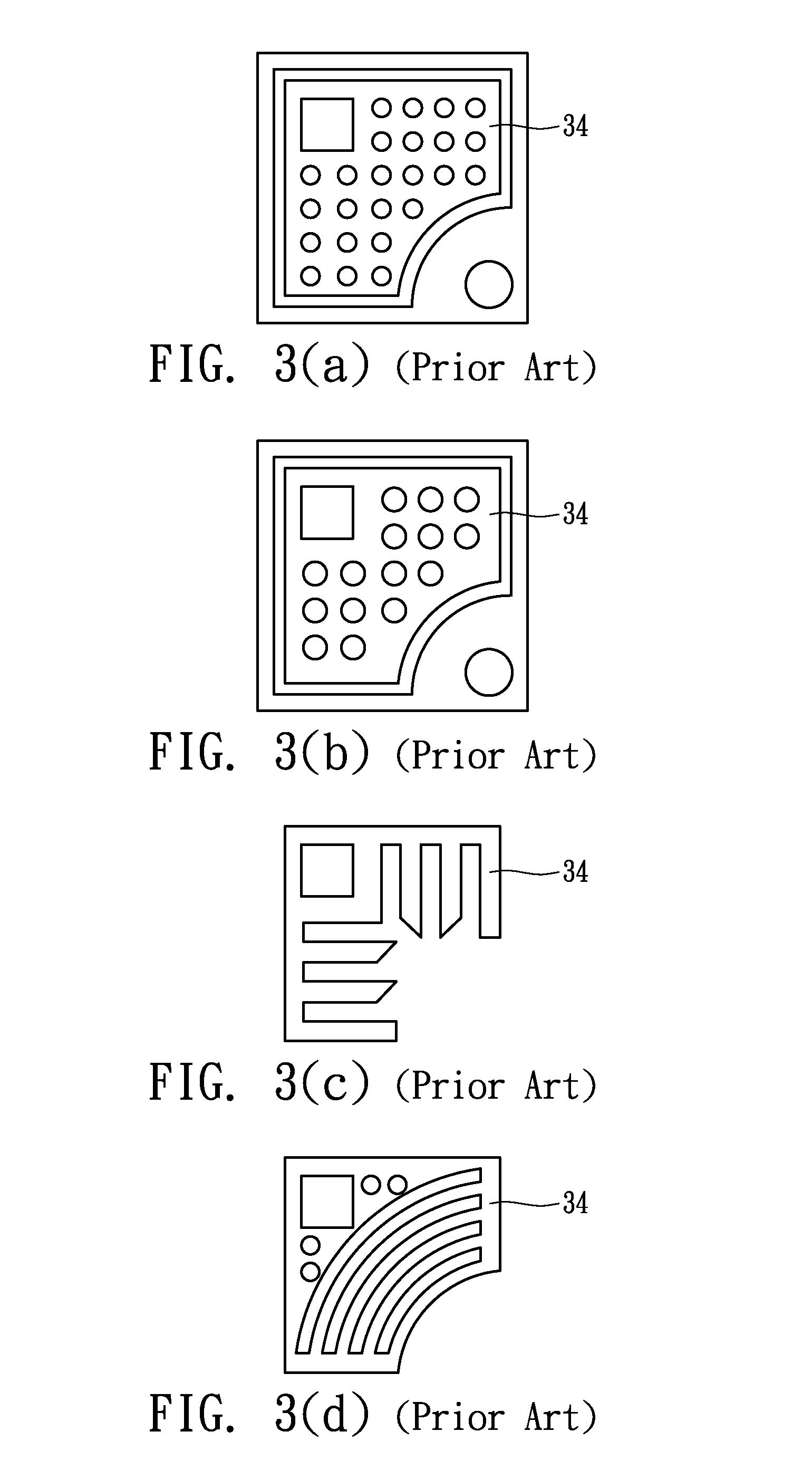
[0019]FIGS. 4-6 show the light-emitting device 110 according to one embodiment of the present invention. The light-emitting device 110 includes a substrate 112, a semiconductor stack structure 120 positioned on the substrate 112, a transparent electrode 126 positioned on a first region 128 of the semiconductor stack structure 120, a plurality of photonic crystals 132 positioned in or on a second region 130 of the semiconductor stack structure 120. The substrate 112 can be made of one material selected from the group consisting of aluminum oxide (sapphire), silicon carbide (SiC), silicon (Si), gallium arsenide (GaAs) and aluminum nitride (AIN).

[0020]The semiconductor stack structure 120 includes an n-type semiconductor layer 114, a p-type semiconductor layer 118 and a light-emitting layer 116 positioned between the n-type semiconductor layer 114 and the p-type semiconductor layer 118. The light-emitting device 110 further includes an n-type electrode 122 positioned on the n-type semi...


PUM


Abstract

A light-emitting device includes a substrate, a semiconductor stacked structure positioned on the substrate, a transparent electrode positioned on a first region of the semiconductor stacked structure, and at least one photonic crystal positioned in a second region of the semiconductor stacked structure. Preferably, the first region surrounds the second region, the area of the first region is larger than that of the second region, and the width of the second region is smaller than 40 micrometers. The structure of photonic crystals can be holes, pillars, continuous protrusions or depressions, discontinuous protrusions or depressions or the combination thereof, and the lattice of photonic crystals can be square, hexagonal, rectangular, periodic, multi-periodic, quasi-periodic or non-periodic.

Description

BACKGROUND OF THE INVENTION[0001](A) Field of the Invention[0002]The present invention relates to a light-emitting device, and more particularly, to a light-emitting device having photonic crystals and a transparent electrode.[0003](B) Description of the Related Art[0004]Low output efficiency of light-emitting devices such as light-emitting diode (LED) originates mainly from low light extraction efficiency, which means that the light actually emitted to the exterior of the light-emitting device is only a small portion of the light generated by the light-emitting layer. To solve this low light extraction efficiency problem of the conventional light-emitting device, researchers try to introduce photonic crystals into the light-emitting device to improve the light extraction efficiency.[0005]FIG. 1 shows a conventional light-emitting device 500 disclosed in U.S. Pat. No. 5,955,749. The light-emitting device 500 includes a dielectric structure 512 consisting of an n-type semiconductor 5...

Claims


Application Information

Patent Timeline
IPC IPC(8): H01S5/00
CPCH01L33/10H01L2933/0083H01L33/38H01L33/20
Inventor HSUEH, HAN TSUNGYEH, WEN YUNGCHI, JIM YONG
Owner IND TECH RES INST
Why Eureka
Try Eureka