Memory device with a managing microprocessor system and an architecture of fail search and automatic redundancy

a microprocessor system and memory device technology, applied in static storage, digital storage, instruments, etc., can solve the problems that the realization of dedicated structures in the device may have a very low impact on the area occupied by the device, and achieve the effects of reducing the time used for executing, reducing the burden on the silicon area, and improving the yield and the productivity of fabrication

a microprocessor system and memory device technology, applied in static storage, digital storage, instruments, etc., can solve the problems that the realization of dedicated structures in the device may have a very low impact on the area occupied by the device, and achieve the effects of reducing the time used for executing, reducing the burden on the silicon area, and improving the yield and the productivity of fabrication

US20080049514A1Active Publication Date: 2008-02-28MICRON TECH INC

Image

  • Memory device with a managing microprocessor system and an architecture of fail search and automatic redundancy
  • Memory device with a managing microprocessor system and an architecture of fail search and automatic redundancy
  • Memory device with a managing microprocessor system and an architecture of fail search and automatic redundancy

Examples


Embodiment Construction

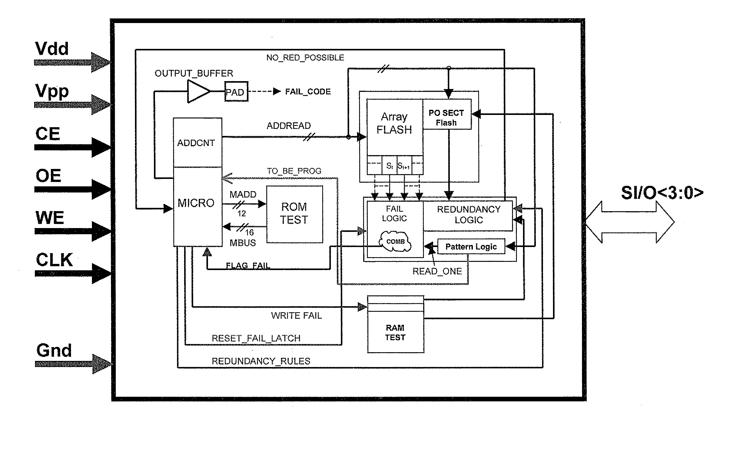
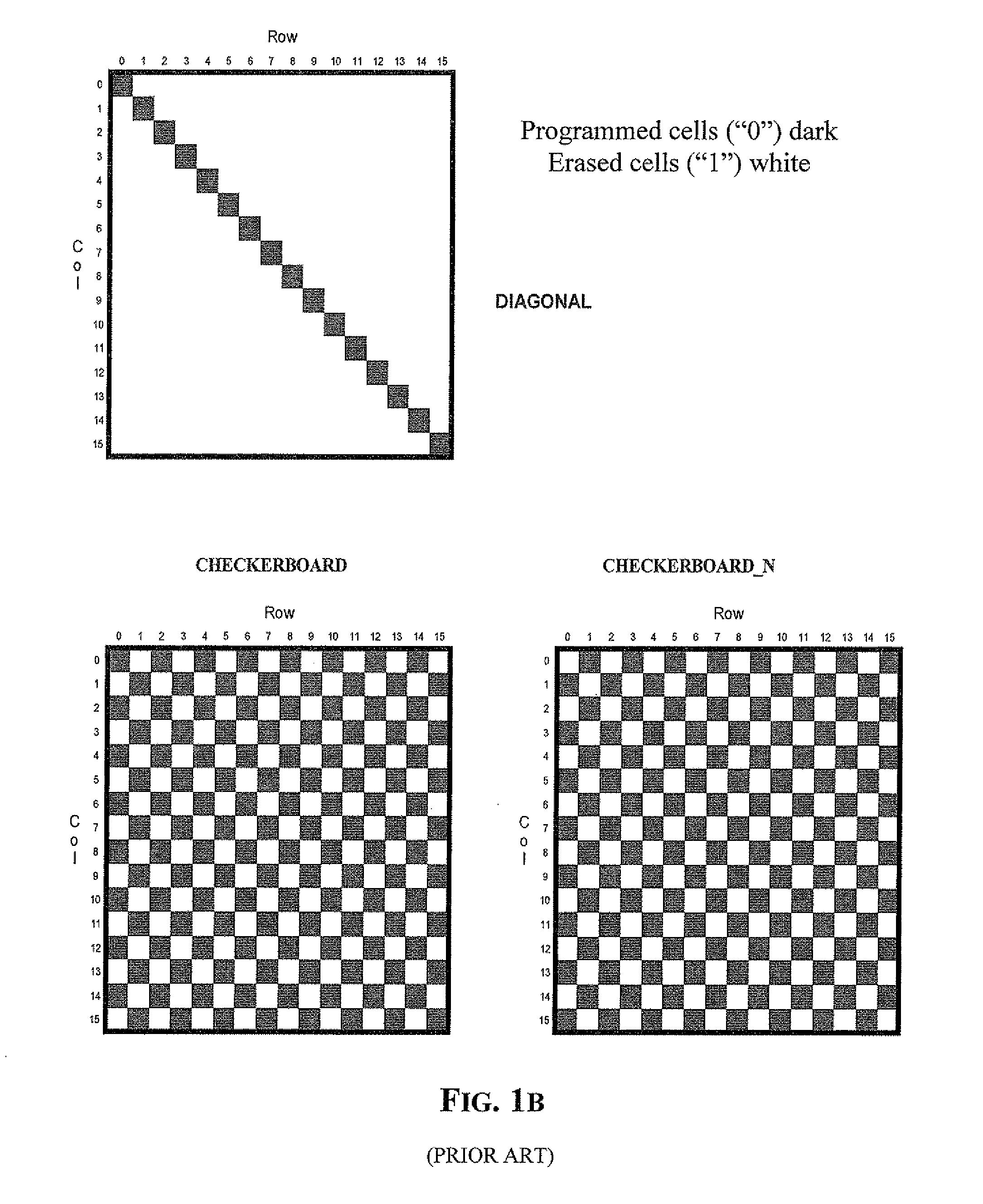
[0018]The process comprises executing a certain set of algorithms, written in an internal ROM, for searching eventual electric failures in the memory cell array. These algorithms comprise two types. The task of the first type of algorithms comprises writing in the array, that is, programming the cells of the array according to a series of specific patterns such as the Checkerboad pattern, the inverted Checkerboard pattern, and the Diagonal pattern, all depicted in FIG. 1B, besides the ALLO pattern. The task of a second type of algorithms comprises verifying, by a read operation, the physical state of the cells of the array in respect to internal reference states for the particular write pattern of the cells and signaling to a logic controller eventual failures (difference between the read value and the expected value) detected during the execution of the verification scanning.

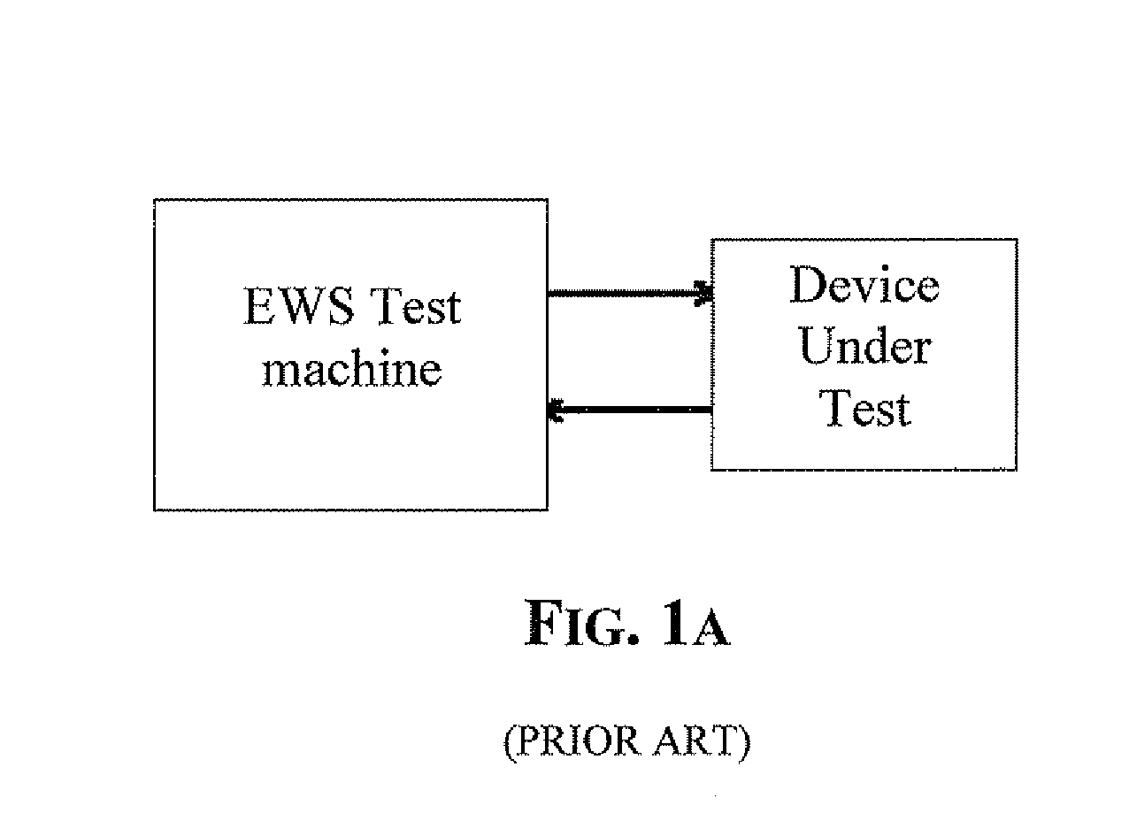
[0019]In practice, it is assumed that the die receive, from the test machine, a single command for starting ...


PUM


Abstract

An automatic redundancy system may exploit an existing microprocessor management system on chip for carrying out autonomously, without communicating with an external testing machine, the operations of: writing data in the memory array according to one or more pre-established test patterns, verifying data successively read from the memory array, and substituting failed elements of the memory array with equivalent redundancy structures. A logic structure may detect and store memory array failures upstream of the output data path. Thereby, data collection relating to failures may be accomplished more quickly and without any interaction with the testing machine apart from communicating the end of the execution of the redundancy process.

Description

FIELD OF THE INVENTION[0001]The invention relates to management of failed memory cells in memory devices, more particularly, FLASH memory devices.BACKGROUND OF THE INVENTION[0002]The market for FLASH memory devices offers small margins for manufacturers of memory devices. The industry is studying new manufacturing techniques and methods to improve both yield and productivity. A known technique for increasing yield comprises implementing row, column, and sector redundancy. These techniques, even if they increase the yield, also increase relatively the time used for testing the devices on wafer, for example, Electric Wafer Sort (EWS). This increase in testing time is because the test machine, besides detecting the physical position of the failed element in the array, may implement a series of procedures for mapping the failed element (row, column, sector) onto an available valid spare resource. This may limit productivity, and for improving it, further investments are made for improvi...

Claims


Application Information

Patent Timeline
28 Feb 2008
Publication
US20080049514A1
IPC
G11C29/12; G11C11/34
CPC
G11C16/04; G11C29/16; G11C29/82; G11C29/48; G11C29/4401
Inventors
MONDELLO, ANTONINO; TUMMINIA, ALESSANDRO