Parallel operation device allowing efficient parallel operational processing

a technology of parallel operation and processing device, which is applied in the direction of program control, computation using denominational number representation, instruments, etc., can solve the problems of insufficient dedicated dsp to achieve dramatic improvement in performance, inability to achieve high speed processing, and large amount of data to be processed, etc., to achieve low degree of parallelism and efficient processing.

Inactive Publication Date: 2008-02-28
RENESAS ELECTRONICS CORP
View PDF13 Cites 8 Cited by
  • Summary
  • Abstract
  • Description
  • Claims
  • Application Information

AI Technical Summary

Benefits of technology

[0016] An object of the present invention is to provide a parallel processing device capable of efficiently performing processes such as arithmetic / logic operation and / or data moving process of low degree of parallelism.
[0021] The parallel processing device, in accordance with the first aspect of the present invention, is configured to set contents of operation in each arithmetic / logic processing element individually, and therefore, operations of low degree of parallelism can be executed concurrently in different entries, whereby performance can be improved. Particularly, data processing can be executed in a closed manner in the processing device, without the necessity of transferring data to the host CPU. Accordingly, the time required for data transfer can be reduced.
[0022] In the parallel processing device in accordance with the second aspect of the present invention, the amount of data movement is set in each entry and data can be moved between entries at a high speed. Accordingly, the time required for data transfer can be reduced.
[0023] In the parallel processing device in accordance with the third aspect of the present invention, contents of operation and data for setting the amount of data movement are stored in each operational processing register of the arithmetic or logic operation. Therefore, a dedicated register is unnecessary, and increase in layout area can be avoided. Further, the amount of data movement and contents of operation are set for each entry, so that high speed processing can be realized.

Problems solved by technology

When the amount of data to be processed is very large, however, even a dedicated DSP is insufficient to attain dramatic improvement in performance.
Therefore, though each process can be done at high speed in an arrangement in which the sum-of-products operation is done using a register file, when the amount of data increases, the time of processing increases in proportion thereto as the data are processed in series, and therefore, such an arrangement cannot achieve high speed processing.
When such a dedicated DSP is used, the processing performance much depends on operating frequency, and therefore, if high speed processing is given priority, power consumption would considerably be increased.
Such successive processing of arithmetic / logic operations with low degree of parallelism hinders increase in processing speed, and hence, the performance of the parallel processing device cannot be fully exhibited.
Therefore, parallel processing of data movement between entries at different distances is impossible.

Method used


Image

  • Parallel operation device allowing efficient parallel operational processing
  • Parallel operation device allowing efficient parallel operational processing
  • Parallel operation device allowing efficient parallel operational processing

Examples


embodiment 1

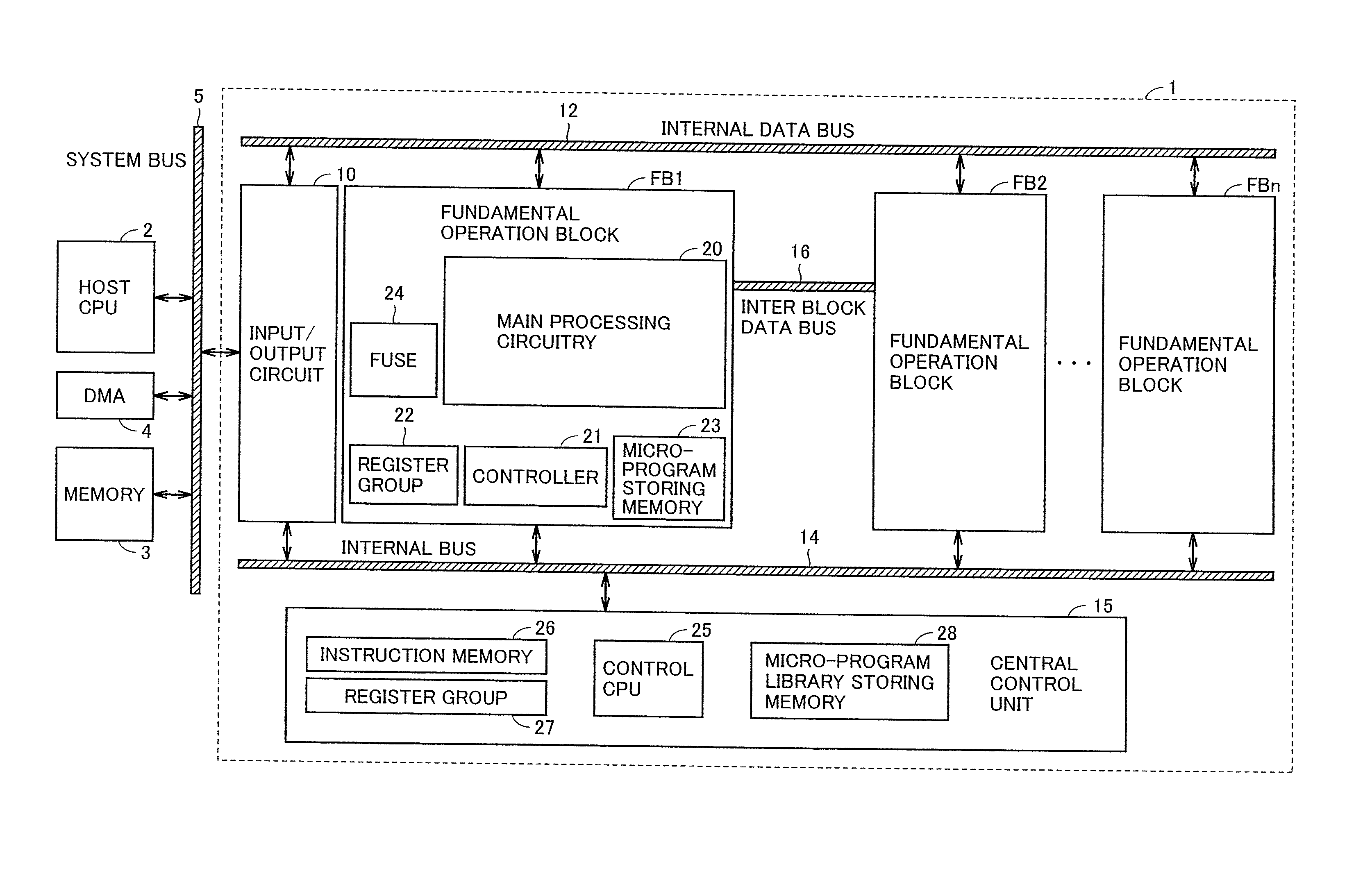
[0078]FIG. 1 schematically shows an overall configuration of a processing system utilizing a semiconductor processing device in accordance with Embodiment 1 of the present invention. Referring to FIG. 1, the processing system includes a semiconductor processing device 1 executing parallel operations; a host CPU 2 performing process control on semiconductor processing device 1, control of the whole system and data processing, a memory 3 used as a main storage of the system and storing various necessary data, and a DMA (Direct Memory Address) circuit 4 directly accessing to memory 3 without handling through host CPU 2. By the control of DMA circuit 4, data can be transferred directly between memory 3 and semiconductor processing device 1, and semiconductor processing device can be accessed directly.

[0079] Host CPU 2, memory 3, DMA circuit 4 and semiconductor processing device 1 are connected with each other through a system bus 5. Semiconductor processing device 1 includes a pluralit...

embodiment 2

[0350]FIG. 49 schematically shows a configuration of an ALU processing element in accordance with Embodiment 2 of the present invention. The configuration of ALU processing element shown in FIG. 49 differs from that of ALU processing element in accordance with Embodiment 1 shown in FIG. 1 in the following point. Specifically, C register 53, F register 54, D register 59 and XL register 58 are used as registers for storing movement control data E0 to E3. In other words, in place of MIMD instruction register (RECM register) 70, operation registers provided in ALU processing element 34 are used. In data movement, an arithmetic operation or a logic operation is not executed, and therefore, XL register 58, D register 59, C register 53 and F register 54 are not used In the data movement operation, these unused registers are utilized as registers for storing movement control data, and hence it becomes unnecessary to provide an MIMD instruction register (RECM register) for this purpose only,...

embodiment 3

[0355]FIG. 50 schematically shows a configuration of the ALU processing element according to Embodiment 3 of the present invention. The ALU processing element shown in FIG. 50 differs from ALU processing element according to Embodiment 1 in the following point. Specifically, as the registers for applying the MIMD instruction to MIMD instruction decoder 74, C register 53 and XL register 58 are used. Except for this point, the configuration of the ALU processing element shown in FIG. 50 is the same as that of the ALU processing element shown in FIG. 10 and therefore, corresponding portions are denoted by the same reference characters and detailed description thereof will not be repeated.

[0356] It is noted, however, that in the configuration shown in FIG. 50 also, multiplexer 150 is provided for inter-ALU communication circuit (RECM) 71, for setting the connection path of inter-ALU communication circuit 71 by switching between the bits E0-E3 from data register (RECM register) 70 and t...


PUM


Abstract

In arithmetic / logic units (ALU) provided corresponding to entries, an MIMD instruction decoder generating a group of control signals in accordance with a Multiple Instruction Multiple Data (MIME) instruction and an MIMD register storing data designating the MIME instruction are provided, and an inter-ALU communication circuit is provided. The amount and direction of movement of the inter-ALU communication circuit are set by data bits stored in a movement data register. It is possible to execute data movement and arithmetic / logic operation with the amount of movement and operation instruction set individually for each ALU unit Therefore, in a Single Instruction-Multiple Data type processing device, Multiple Instruction-Multiple Data operation can be executed at high speed in a flexible manner.

Description

BACKGROUND OF THE INVENTION [0001] 1. Field of the Invention [0002] The present invention relates to a semiconductor processing device and, more specifically, to a configuration of a processing circuit performing arithmetic / logic operations on a large amount of data at high speed using semiconductor memories. [0003] 2. Description of the Background Art [0004] Recently, along with wide spread use of portable terminal equipment, digital signal processing allowing high speed processing of a large amount of data such as voice data and image data comes to have higher importance. For such digital signal processing, generally, a DSP (Digital Signal Processor) is used as a dedicated semiconductor device. Digital signal processing of voice and image includes data processing such as filtering, which in turn frequently requires arithmetic operations with repetitive sum-of-products operations. Therefore, a DSP is generally configured to have a multiplication circuit, an adder circuit and a regi...

Claims


Application Information

Patent Timeline
Patent Type & Authority Applications(United States)
IPC IPC(8): G06F9/302G06F9/305
CPCG06F9/30036G06F9/3887G06F9/3879
Inventor SUEYOSHI, TOSHINORIIIDA, MASAHIRONAKANO, MITSUTAKASENOUE, FUMIAKIMIZUMOTO, KATSUYA
Owner RENESAS ELECTRONICS CORP
Why Eureka
Try Eureka