Nitride semiconductor substrate and method of manufacturing the same

a technology of nitride and semiconductor substrate, which is applied in the direction of semiconductor/solid-state device manufacturing, semiconductor devices, electrical equipment, etc., can solve the problems of linear defects and dislocations of gan layers growing on heterogeneous substrates, and achieve the effect of reducing manufacturing costs

Inactive Publication Date: 2008-03-06
IND TECH RES INST
View PDF16 Cites 11 Cited by
  • Summary
  • Abstract
  • Description
  • Claims
  • Application Information

AI Technical Summary

Benefits of technology

[0009]The present invention is directly to a manufacturing method of a nitride semiconductor substrate so as to reduce the manufacturing cost.

Problems solved by technology

For example, a mixture of blue and yellow phosphors made of gallium nitride (GaN) is capable of generating white light, which leads to a higher luminance and substantially lower power consumption than a conventional light bulb.
However, since aluminum oxide substrate itself is different from GaN series in lattice constant, thermal expansion coefficients and chemical properties, the GaN layer growing on a heterogeneous substrate (e.g. a silicon substrate, a silicon carbide substrate, or an aluminum oxide substrate) may have linear defects and dislocations.
The dislocations extend together with the increasing thickness of the growing GaN layer, resulting in the formation of threading dislocations.
The foresaid defects would affect the laser performance of the ultraviolet LEDs and of the GaN-series compound and reduce their lifetime.
However, the barrier structures 104 are formed through at least once performance of photolithography and etching process, and vacuum apparatuses are also required to this manufacturing process; thus, the steps are more complicated and the cost is higher.
Similar to the barrier structures 104 illustrated in FIG. 1, the trenches 206 passing through the buffer layer 202 and the seed layer 204 are formed through at least once performance of photolithography and etching process, and vacuum apparatuses are also required for the manufacturing process; thus these steps are more complicated and the cost is higher.

Method used


Image

  • Nitride semiconductor substrate and method of manufacturing the same
  • Nitride semiconductor substrate and method of manufacturing the same
  • Nitride semiconductor substrate and method of manufacturing the same

Examples


Embodiment Construction

[0022]Reference will now be made in detail to the present preferred embodiments of the invention, examples of which are illustrated in the accompanying drawings. Wherever possible, the same reference numbers are used in the drawings and the description to refer to the same or like parts.

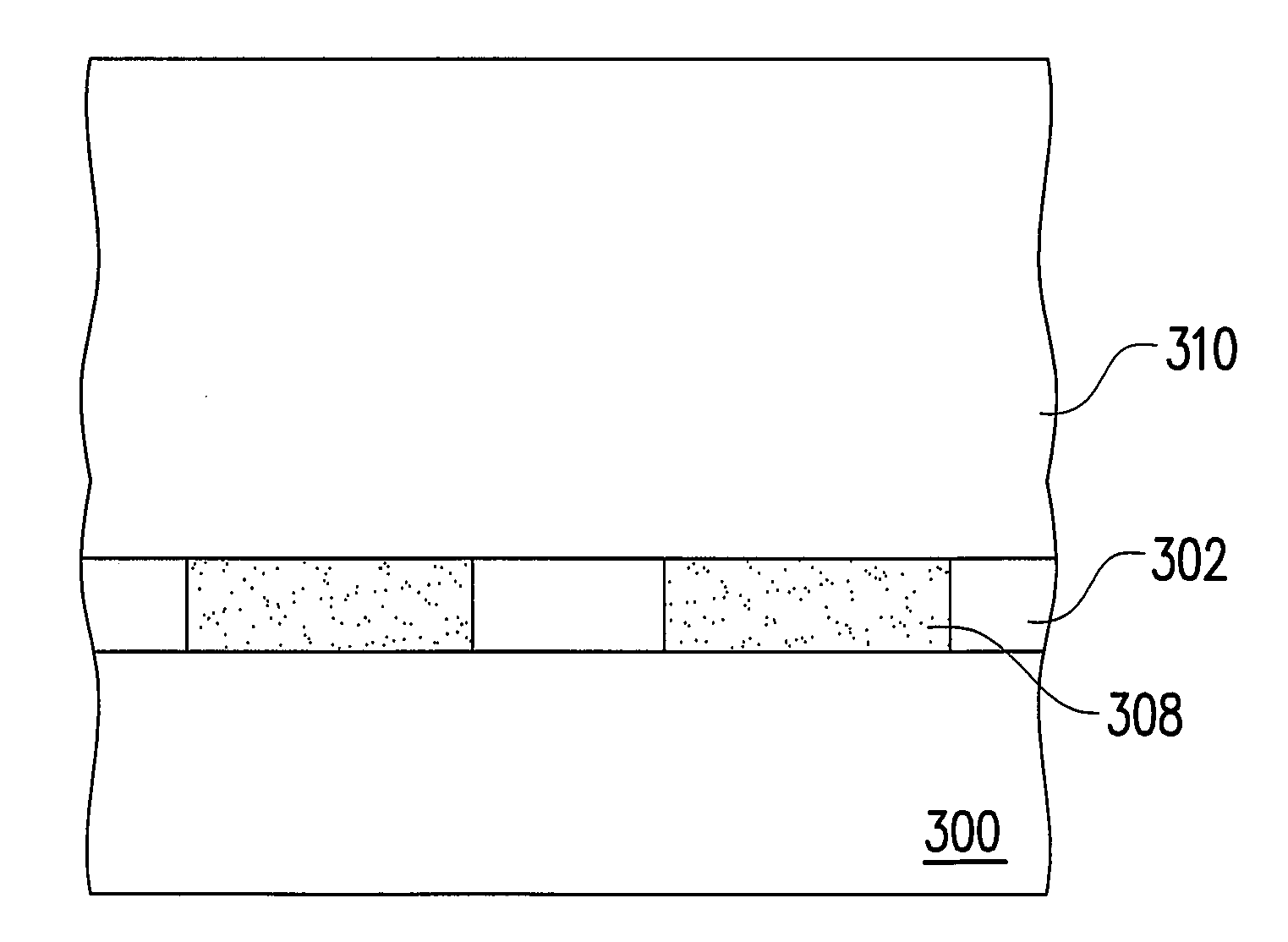
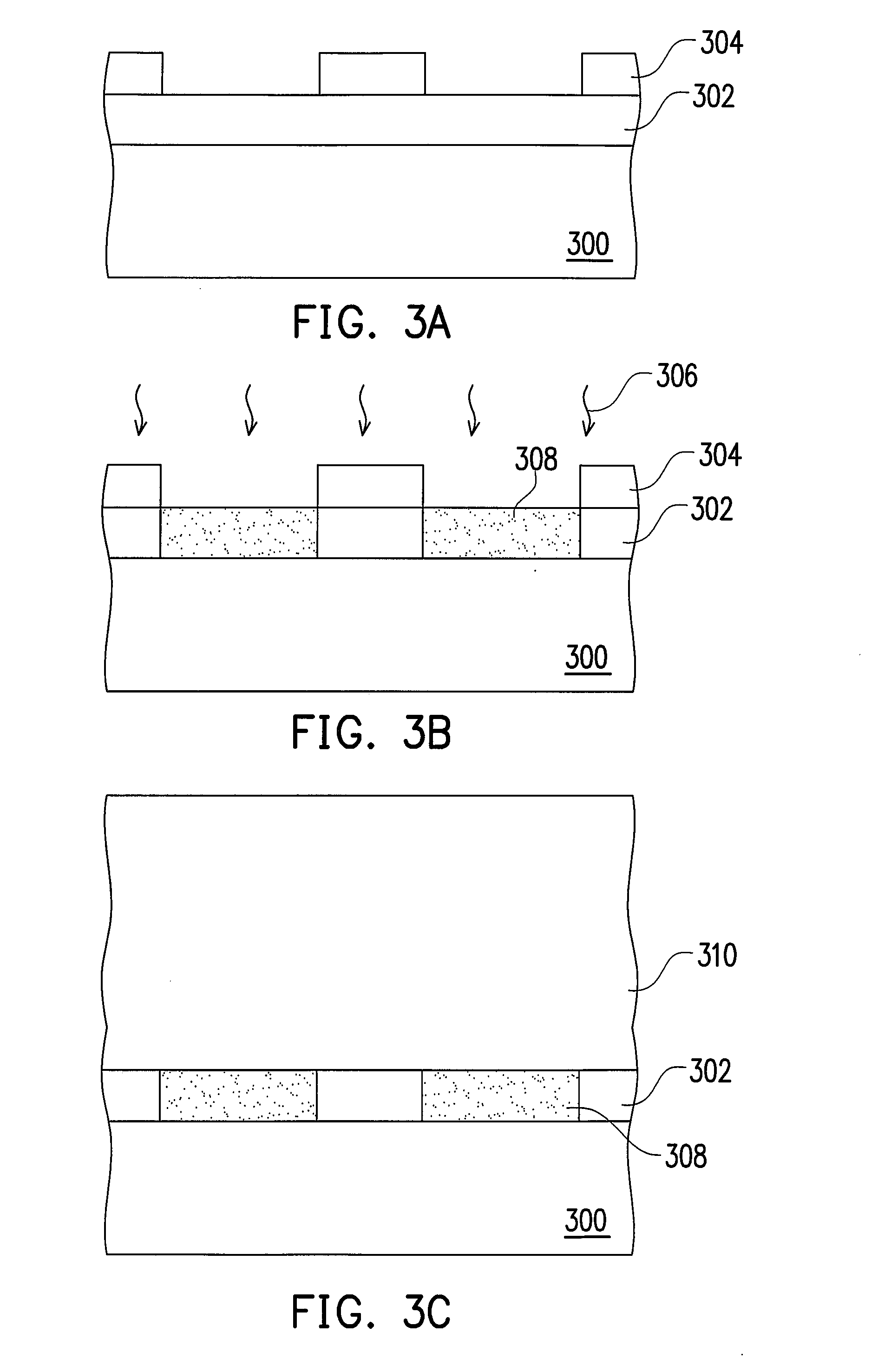
[0023]FIGS. 3A to 3C depict a manufacturing method of a nitride semiconductor substrate according to one preferred embodiment of the present invention.

[0024]Firstly, refer to FIG. 3A, a substrate 300 is provided. Next, an epitaxy layer 302 is formed on the substrate 300. Next, a patterned mask layer 304 is formed on the epitaxy layer 302. The patterned mask layer 304 exposes a portion of the epitaxy layer 302. The patterned mask layer 304 is, for example, a photoresist layer. Then, refer to FIG. 3B, an oxidation process 306 is performed by using the patterned mask layer 304 as a mask to completely oxidize the exposed epitaxy layer 302 to form a plurality of blocking structures 308, namely the disloca...


PUM

PropertyMeasurementUnit
temperatureaaaaaaaaaa
semiconductoraaaaaaaaaa

Abstract

The present invention relates to a method of forming a nitride semiconductor substrate. This method includes steps of providing a substrate and then forming an epitaxy layer on the substrate. A patterned mask layer is formed on the epitaxy layer, wherein the patterned mask layer exposes a portion of the epitaxy layer. Next, an oxidation process is performed to oxidize the exposed epitaxy layer so as to form a plurality of dislocation blocking structures. The patterned mask layer is then removed. Further, a nitride semiconductor layer is formed on the epitaxy layer having the dislocation blocking structures.

Description

CROSS-REFERENCE TO RELATED APPLICATION[0001]This application claims the priority benefit of Taiwan application serial no. 95132698, filed Sep. 5, 2006. All disclosure of the Taiwan application is incorporated herein by reference.BACKGROUND OF THE INVENTION[0002]1. Field of the Invention[0003]The present invention relates to a semiconductor substrate of group III-V and a method of manufacturing the same, and more particularly to a nitride semiconductor substrate and a method of manufacturing the same.[0004]2. Description of Related Art[0005]In the recent years, light emitting diodes (LED) and laser diodes (LD) have been prevailing in commercial use. For example, a mixture of blue and yellow phosphors made of gallium nitride (GaN) is capable of generating white light, which leads to a higher luminance and substantially lower power consumption than a conventional light bulb. In addition, the LED has a lifetime of more than tens of thousand hours, longer than that of conventional light ...

Claims


Application Information

Patent Timeline
Patent Type & Authority Applications(United States)
IPC IPC(8): H01L33/00
CPCH01L21/0237H01L21/02458H01L21/02463H01L21/02647H01L21/02639H01L21/02642H01L21/0254
Inventor LAI, CHIH-MINGTSAY, JENQ-DARLIU, WEN-YUEHGUO, YIH-DER
Owner IND TECH RES INST
Why Eureka
Try Eureka