Inspection Equipment of Circuit Board and Inspection Method of Circuit Board
a circuit board and inspection equipment technology, applied in the direction of resistance/reactance/impedence, measurement devices, instruments, etc., can solve the problems of difficult to infix a large number of metallic pins into the board at a high density, the electrode of the circuit board to be inspected is apt to be damaged, and the inspection equipment is difficult to achieve high reliability, excellent follow-up, and accurate inspection
- Summary
- Abstract
- Description
- Claims
- Application Information
AI Technical Summary
Benefits of technology
Problems solved by technology
Method used
Image

Examples
example 1
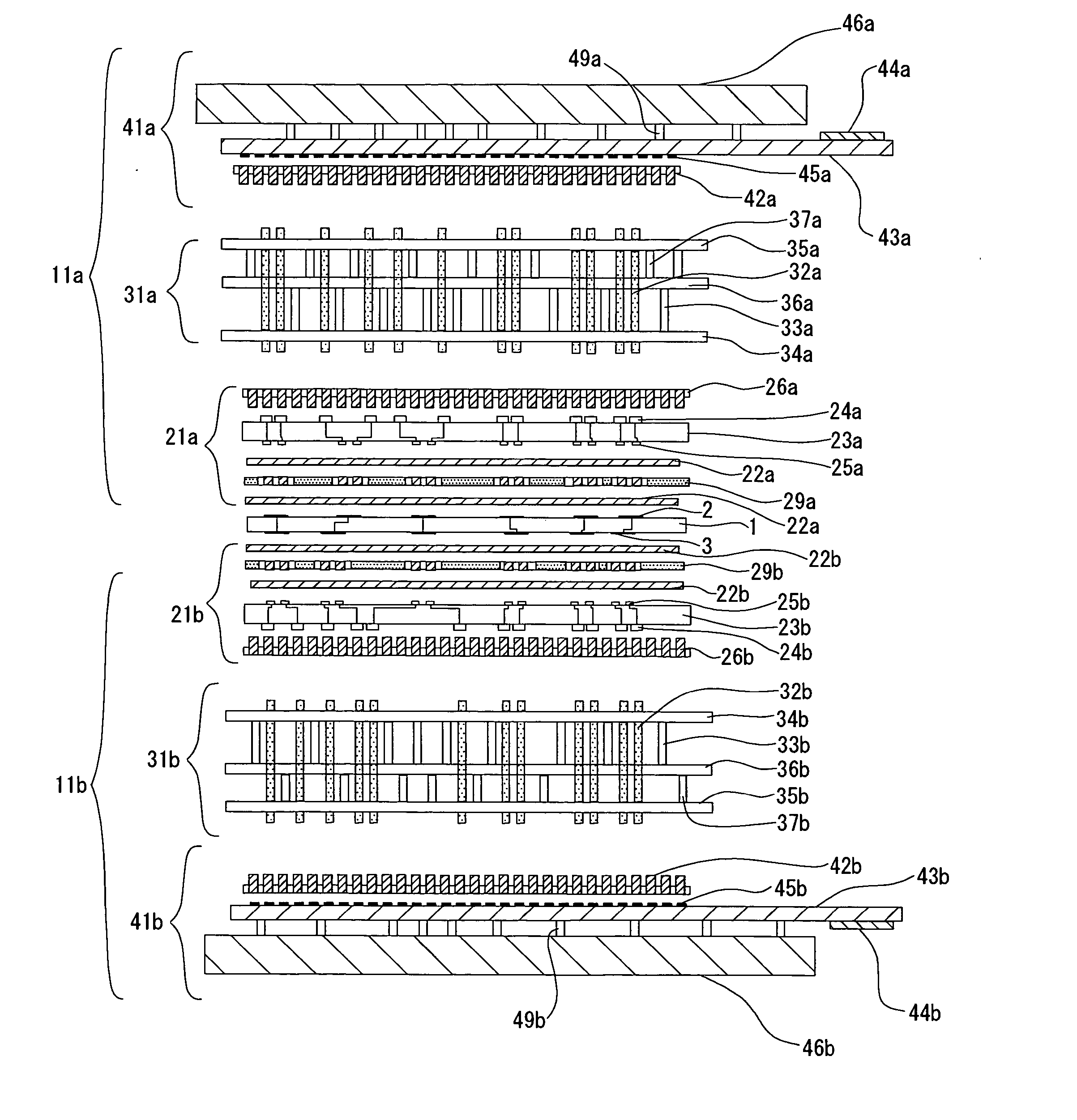
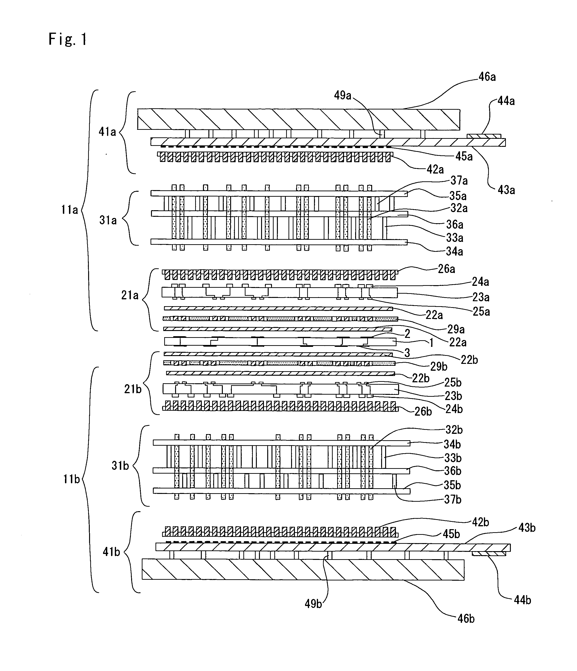
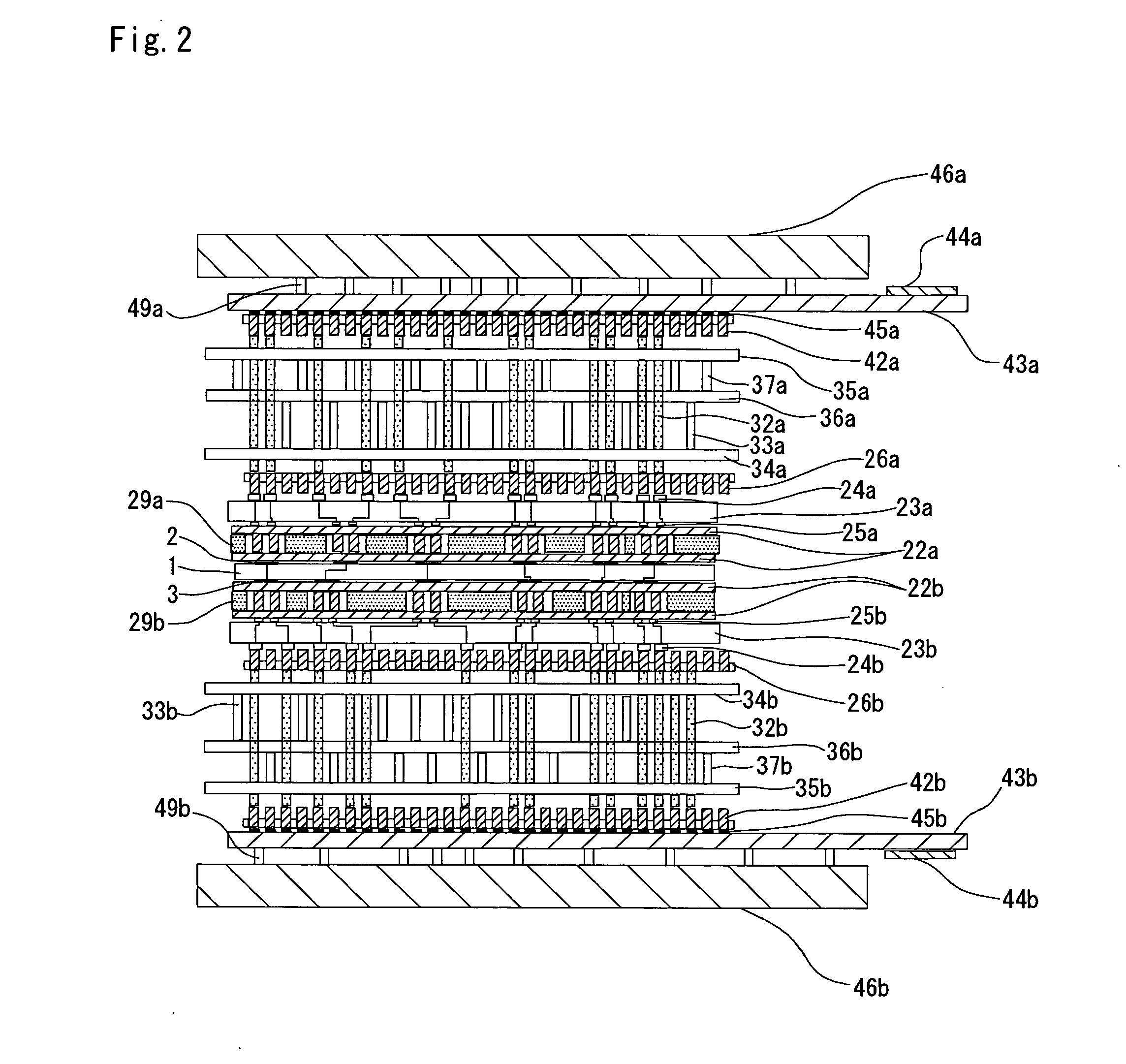
[0397] There was fabricated an inspecting apparatus for inspecting the following circuit board for estimation shown in FIG. 1 which is adapted to the inspecting portion of a rail delivery type circuit board automatic inspecting machine (manufactured by Nidec Read Corporation, trade name: STARREC V5).
(1) Circuit Board 1 for Estimation
[0398] A circuit board 1 for estimation which has the following specification was prepared.
[0399] Dimension: 100 mm (length)×100 mm (width)×0.8 mm (thickness)
[0400] Number of electrodes to be inspected on upper surface side: 3600
[0401] Diameter of electrode to be inspected on upper surface side: 0.25 mm
[0402] Minimum arrangement pitch of electrode to be inspected on upper surface side: 0.4 mm
[0403] Number of electrodes to be inspected on lower surface side: 2600
[0404] Diameter of electrode to be inspected on lower surface side: 0.25 mm
[0405] Minimum arrangement pitch of electrode to be inspected on lower surface side: 0.4 mm
(2) First Anisotro...
example 2
[0464] The relay board 29 in the inspecting apparatus according to the example 1 was changed into that shown in FIG. 12. First of all, the relay board 29a for the first inspecting jig 11a having 7200 electrode structures was manufactured in the following manner.
[0465] There was prepared the laminating material 90A (manufactured by Nippon Steel Chemical Co., Ltd.: Espanex LC18-50-00NE) obtained by integrally laminating the metal layer 93A formed of copper having a thickness of 18 μm over one surface of the insulating board 91 formed of a liquid crystal polymer having a thickness of 50 μm (FIG. 14), and a dry film resist was laminated on the metal layer in the laminating material to form a resist film.
[0466] Subsequently, the resist film thus formed was subjected to an exposing treatment and a developing treatment so that a circular pattern hole having a diameter of 40 μm was formed on the resist film in accordance with a pattern corresponding to the electrode to be inspected on the...
PUM
 Abstract
Description
Claims
Application Information