Method for Manufacturing Semiconductor Device

a manufacturing method and semiconductor technology, applied in the direction of semiconductor devices, basic electric elements, electrical appliances, etc., can solve the problems of monetary burden but also time delay risk, extreme cost, and inability to manufacture, so as to reduce the time loss due to the replacement of photomasks, and reduce the cost of manufacturing

Active Publication Date: 2008-03-06
SEMICON ENERGY LAB CO LTD
View PDF26 Cites 41 Cited by
  • Summary
  • Abstract
  • Description
  • Claims
  • Application Information

AI Technical Summary

Benefits of technology

[0010]Accordingly, the present invention offers a method for forming an opening portion by a simple process without using a photomask or a resist. Further, the present invention proposes a method for manufacturing a semiconductor device at low cost.
[0019]By irradiating the plurality of light absorbing layers with a laser beam such as a linear laser beam or a rectangular laser beam, the plurality of light absorbing layers can be irradiated with a laser beam at one time, and accordingly, semiconductor devices can be manufactured with high mass productivity.
[0020]Thus, an opening portion can be formed without using a resist or a photomask, which are required in a conventional photolithography technique. Since a photomask is not used, time loss due to replacement of photomasks can be reduced, and accordingly, the limited production of diversified products is possible. Further, since a resist and a developing solution for the resist are not used, a large amount of a chemical solution and water are not required. Therefore, the process can be greatly simplified and cost can be reduced compared with a process of forming an opening portion using a conventional photolithography technique.
[0021]By using the present invention, a process of contact opening in a semiconductor device can be performed by a simple process. Further, a method for manufacturing a semiconductor device can be provided at low cost.

Problems solved by technology

However, photomasks used in photolithography techniques have a detailed shape, and a high degree of precision is required for their shape; therefore, they are extremely expensive.
As described above, since a photomask is a shaped object which is formed with a detailed shape to a high degree of precision, it takes considerable time to manufacture.
That is, if the replacement of a photomask which accompanies a change in design or an imperfection in design, results in not only a monetary burden but also the risk of time delay.
Further, since a resist and a developing solution for a resist are used in a step of forming an opening portion in a photolithography step, there is a problem in that a large amount of a chemical solution and water are required and it is necessary to dispose of a large amount of a waste solution.

Method used


Image

  • Method for Manufacturing Semiconductor Device
  • Method for Manufacturing Semiconductor Device
  • Method for Manufacturing Semiconductor Device

Examples


embodiment mode 1

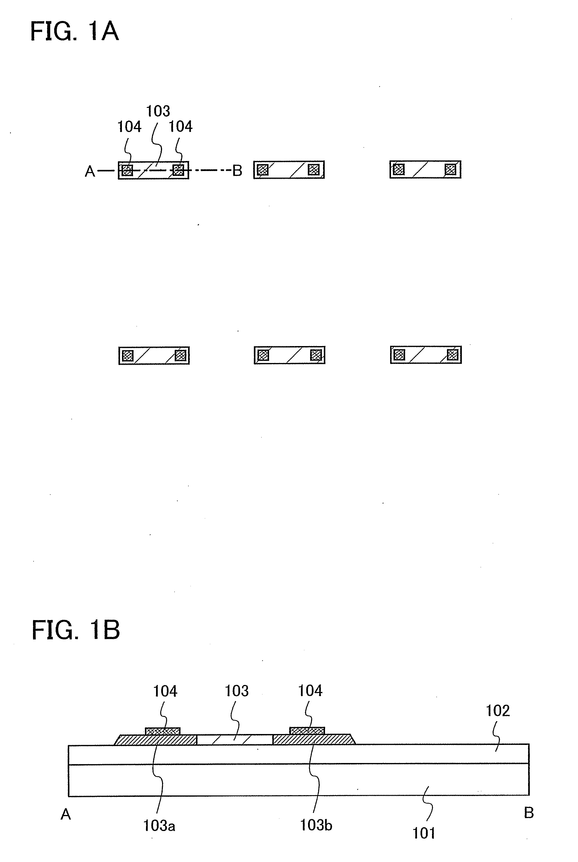
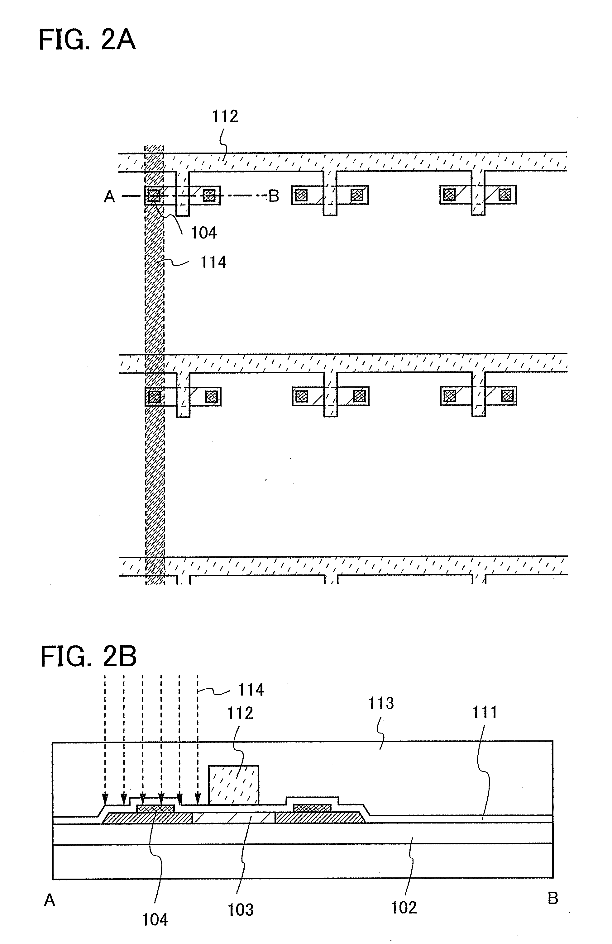
[0048]In this embodiment mode, a LAP (Laser Ablation Process), in which an opening portion is formed by laser beam irradiation without undergoing a photolithography step, is shown hereinafter. FIGS. 1A to 5B are top views and cross-sectional views showing a step of forming an opening portion in an insulating layer formed over a substrate, in a pixel portion in which pixels each including a display element are arranged in matrix. FIGS. 1B, 2B, 3B, 4B, and 5B show cross-sectional views taken along lines A-B of FIGS. 1A, 2A, 3A, 4A, and 5A, respectively.

[0049]In this embodiment mode, description is made with reference to a mode in which a top-gate thin film transistor is used as a thin film transistor that is part of a display element and an opening portion is formed in an insulating layer formed over a semiconductor layer of the thin film transistor. However, the present invention is not limited to this and is appropriately applicable to a mode in which an opening portion is formed in...

embodiment mode 2

[0104]This embodiment mode describes a method for forming an opening portion in an insulating layer formed over a substrate by a process different from that in Embodiment Mode 1 in a pixel portion in which pixels each including a display element are arranged in matrix, with reference to FIGS. 6A to 10B. This embodiment mode is different from Embodiment Mode 1 in a step of removing a light absorbing layer by a laser beam. FIGS. 6A to 10B are top views and a cross-sectional views each illustrating a step of forming an opening portion in an insulating layer formed over a substrate. FIGS. 6B, 7B, 8B, 9B, and 10B show cross-sectional views taken along lines A-B in FIGS. 6A, 7A, 8A, 9A, and 10A, respectively.

[0105]In this embodiment mode, description is made with reference to a mode in which a plurality of light absorbing layers in a direction intersecting with a source wiring is irradiated with a linear laser beam in a pixel portion in which pixels which each include a display element ar...

embodiment 1

[0122]In this embodiment, a liquid crystal display device which is an example of a semiconductor device is described with reference to FIGS. 11A to 11C.

[0123]As shown in FIG. 11A, thin film transistors 225 to 227 are formed over a substrate 101. As a method for forming an opening portion which connects wirings 234 to 239 of the thin film transistors 225 to 227 and a semiconductor film, the above-described embodiment mode can be employed. In this embodiment, each gate electrode of the thin film transistors 225 to 227 is formed to have a two-layer structure. Here, after a tantalum nitride film with a thickness of 30 nm and a tungsten film with a thickness of 370 nm are formed over the gate insulating film by a sputtering method, a resist mask formed by a photolithography step is used to etch the tantalum nitride film and the tungsten film selectively, and the gate electrodes each having a shape that an end portion of the tantalum nitride film extends out farther to the outside than an...


PUM


Abstract

The present invention offers a method for forming an opening portion by a simple process without using a photomask or a resist. Further, the present invention proposes a method for manufacturing a semiconductor device at low cost. A plurality of light absorbing layers is formed over a substrate, an interlayer insulating layer is formed over the plurality of light absorbing layers, the plurality of light absorbing layers is irradiated with a linear or rectangular laser beam from the interlayer insulating layer side, and at least the interlayer insulating layer which is over the plurality of light absorbing layers is removed and an opening portion is formed; and accordingly, a plurality of opening portions can be formed by removing the plurality of light absorbing layers and an insulating film formed over the plurality of light absorbing layers.

Description

BACKGROUND OF THE INVENTION[0001]1. Field of the Invention[0002]The present invention relates to a method for manufacturing a semiconductor device including a semiconductor element having an opening portion.[0003]2. Description of the Related Art[0004]Conventionally, so-called active matrix driving type display panels or semiconductor integrated circuits which have a semiconductor element typified by a thin film transistor (hereinafter also referred to as a “TFT”) or a MOS (Metal Oxide Semiconductor) transistor are manufactured by forming a resist mask formed by a light-exposure step (hereinafter referred to as a photolithography step) which uses a photomask, and selectively etching various thin films, whereby opening portions are formed.[0005]In a photolithography step, a resist mask is formed by applying a resist to an entire surface of a substrate, prebaking it, irradiating the resist with ultraviolet rays or the like through a photomask and exposing the resist, and then developi...

Claims


Application Information

Patent Timeline
Patent Type & Authority Applications(United States)
IPC IPC(8): H01L21/84
CPCH01L27/1214H01L27/1288
Inventor ARAI, YASUYUKITANAKA, KOICHIROSUZUKI, YUKIE
Owner SEMICON ENERGY LAB CO LTD
Why Eureka
Try Eureka