

Selective area deposition and devices formed therefrom
a technology of selective area and thin film, applied in the direction of resistive material coating, thin/thick film capacitor, coating, etc., can solve the problem that the entire circuitry device may be even smaller, and achieve the effect of fewer processing steps, fine resolution and economic benefits
Inactive Publication Date: 2008-03-06
NGIMAT CO
View PDF1 Cites 19 Cited by
- Summary
- Abstract
- Description
- Claims
- Application Information
AI Technical Summary
Benefits of technology
[0012]The masking procedure of the present invention involves substantially fewer processing steps than photolithographic processes. In forming printed circuitry, even if resolution is sacrificed to some extent, economic benefits may be realized. Furthermore, because of the flexibility in forming devices with multiple layers of patterned circuitry components, even if resolution is lost in some cases, an entire circuitry device may be even smaller than is practically achievable by such devices produced by photolithographic processes.
[0014]Alternative masks include photoresist on the substrate prior to deposition, ink printing techniques, e.g., ink jet, and blank masking with selective area removal via photons or electrons, e.g., laser, x-ray, etc. ablation. Such techniques may produce very fine resolution.
[0015]A further advantage of the present technique is the accuracy and precision that are inherent to devices formed that do not require post processing (i.e. etching). As the material forming the device (for example, resistive material for resistors), is deposited, the desired characteristic (i.e. resistance) can be measured either continuously, or periodically. Once the desired value is achieved, the deposition is terminated. As no etching of the material is required, this value remains the same, resulting in a method to produce resistors or other components with improved accuracy and reduced manufacturing and processing costs, when compared to other methods of forming accurate components (such as laser trimming).
Problems solved by technology
Furthermore, because of the flexibility in forming devices with multiple layers of patterned circuitry components, even if resolution is lost in some cases, an entire circuitry device may be even smaller than is practically achievable by such devices produced by photolithographic processes.
Method used
View moreImage
Smart ImageViewing Examples


Examples
example 1
[0064]On a copper surface, a thin film of platinum was deposited by combustion chemical vapor deposition (CCVD) according to the method taught in U.S. Pat. No. 5,652,021. Inadvertently, a finger print was left on the copper surface. The platinum deposited uniformly on the surface, except where the finger print was left; no platinum deposited on the oily surfaces of the print.
Login to View More PUM
| Property | Measurement | Unit |
|---|---|---|
| thick | aaaaa | aaaaa |
| thick | aaaaa | aaaaa |
| thickness | aaaaa | aaaaa |
Abstract
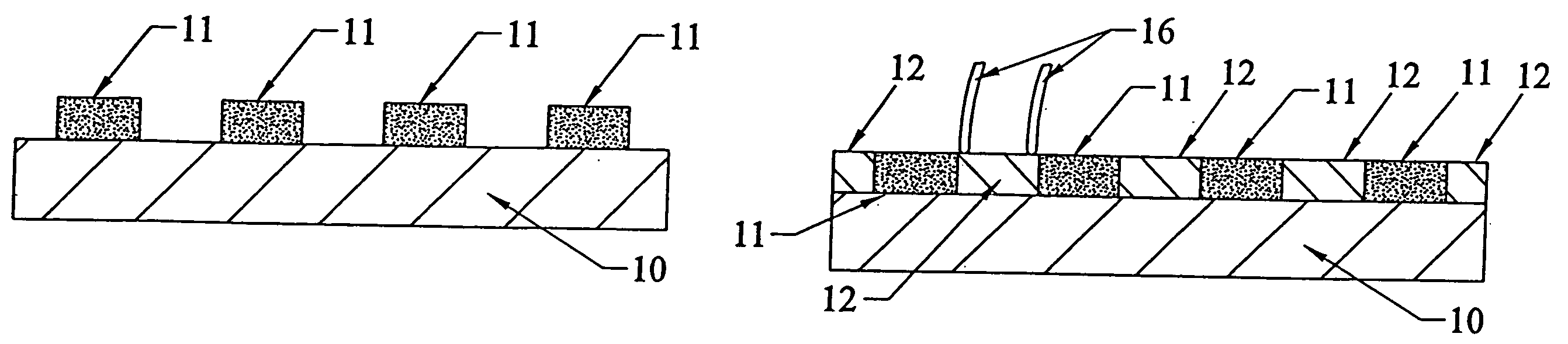
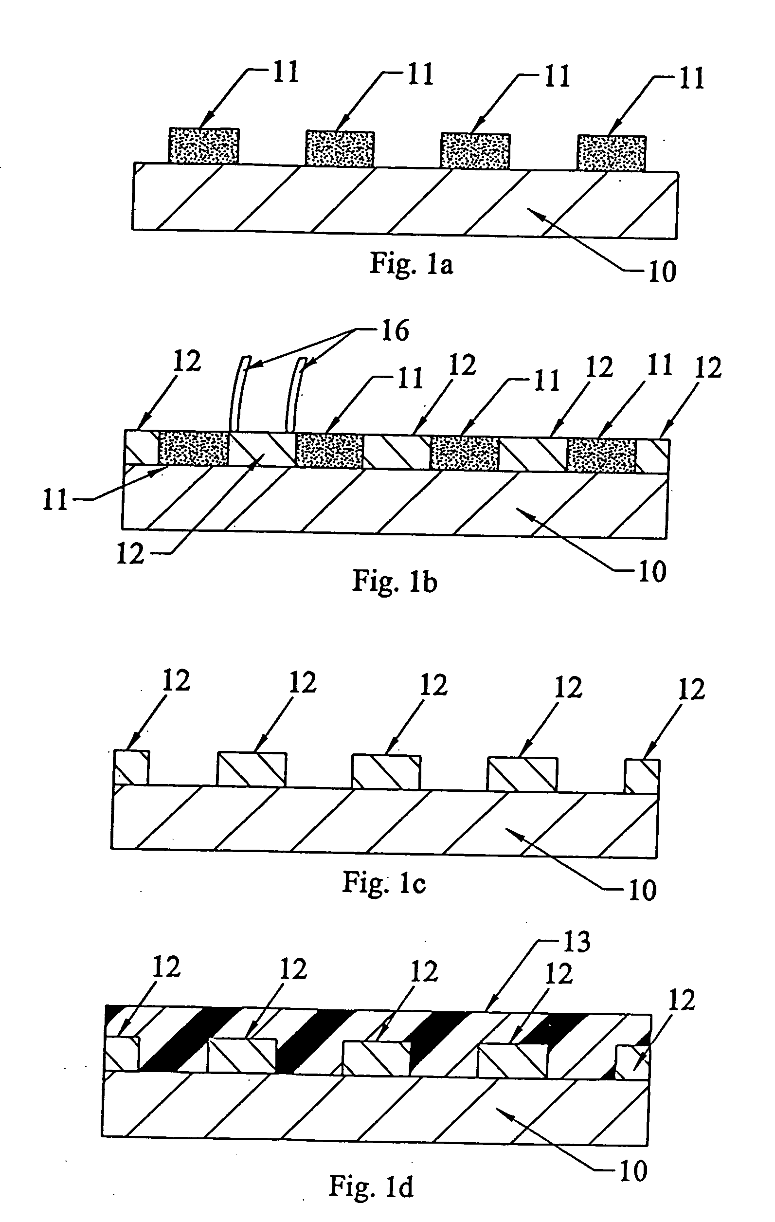
Patterned thin film layers (12) are applied to a substrate (10) surface by masking selective areas of a substrate surface, e.g., with a printed pattern (11) of a material such as an oil, and vapor-depositing thin film material. The masking material is subsequently removed.
Description
FIELD OF THE INVENTION[0001]The present invention is directed to selective area deposition of thin films, including, but not limited, to thin films useful for forming electronic circuitry.BACKGROUND OF THE INVENTION[0002]Circuitry traces of printed electronic circuitry are typically formed by a photolithographic process. In a typical process for forming a layer of circuitry traces, a blank is prepared comprising a metal layer, typically copper, on a dielectric substrate, such as a fiberglass-epoxy composite. A layer of photoresist is applied to the metal layer, and patterned artwork laid over the photoresist layer. Then the photoresist is exposed to actinic radiation so as to affect the exposed portions of the photoresist. Then the photoresist is developed with an appropriate developing solution that washes away exposed portions of the photoresist, in the case of negative-acting photoresists, and non-exposed portions, in the case of positive-acting photoresists. Next, the metal laye...
Claims
Login to View More Application Information
Patent Timeline
 Patent Type & AuthorityApplications(United States)
IPC IPC(8): H01L21/20
CPCC23C16/042C23C16/453H05K3/143H01C17/08H01G4/33H01C7/006
InventorHUNT, ANDREW T.HWANG, JAN TZYY-JIUAN
OwnerNGIMAT CO