Flip chip substrate structure and the method for manufacturing the same

a technology of flip chip and substrate, applied in the direction of printed circuit manufacturing, printed circuit aspects, non-metallic protective coating applications, etc., can solve the problems of reduced substrate thickness, increased process complexity, low integration, etc., and achieve the effect of reducing the thickness of the substra

Inactive Publication Date: 2008-03-13
PHOENIX PRECISION TECH CORP
View PDF5 Cites 75 Cited by
  • Summary
  • Abstract
  • Description
  • Claims
  • Application Information

AI Technical Summary

Benefits of technology

[0008]In view of the foregoing disadvantages, the object of the present invention is to provide a flip ch

Problems solved by technology

Though a high pin quantity can be obtained, operations at higher frequencies or speeds are restricted due to unduly long lead routes and consequent limited performance.
Besides, multiple connection interfaces are required in conventional packaging, leading to increased process com

Method used


Image

  • Flip chip substrate structure and the method for manufacturing the same
  • Flip chip substrate structure and the method for manufacturing the same
  • Flip chip substrate structure and the method for manufacturing the same

Examples


example 1

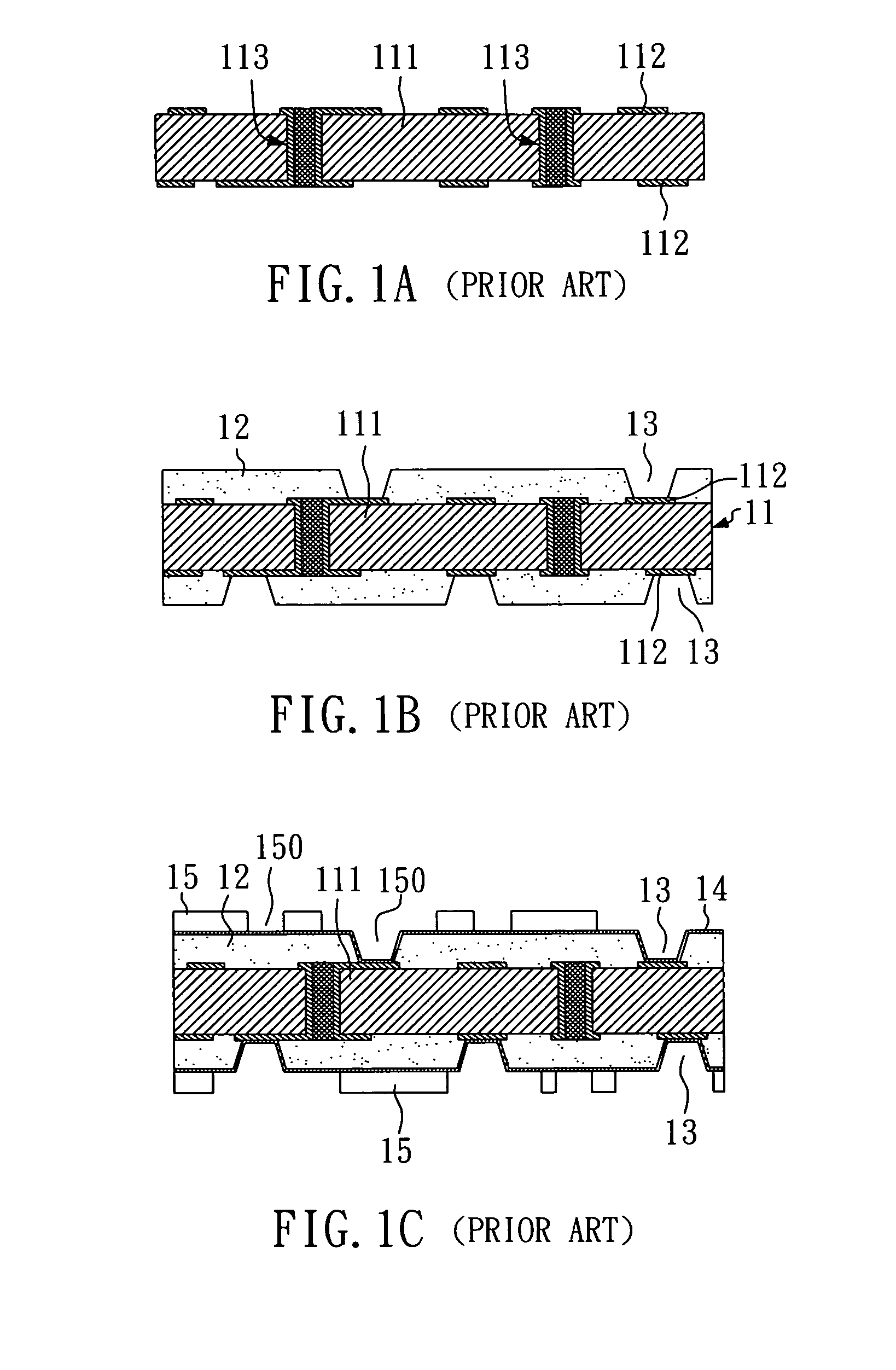
[0035]FIGS. 2A-2Q illustrate the cross-section of one embodiment of the flip chip substrate structure of the present invention. First, as shown in FIG. 2A, a carry board is provided, which is a metal plate, preferably a copper plate. Then, as shown in FIG. 2B, a first solder mask 202 is coated on the carry board 201, and plural first openings 203 are formed by exposure and development, as shown in FIG. 2C. A conductive metal layer 204, an etching-stop layer 205 and a metal layer 206 are formed orderly upward by electroplating or electroless plating, as shown in FIGS. 2D-2F, wherein the materials of the conductive metal layer 204 and the metal layer 206 are copper, and the material of the etching-stop layer 205 is at least one selected from the group consisting of iron, nickel, chromium, titanium, aluminum, silver, tin, lead or the alloys thereof.

[0036]Referring to FIG. 2G, a dielectric layer 208 is formed on the surfaces of the metal layer 206 and the first solder mask 202, wherein ...

example 2

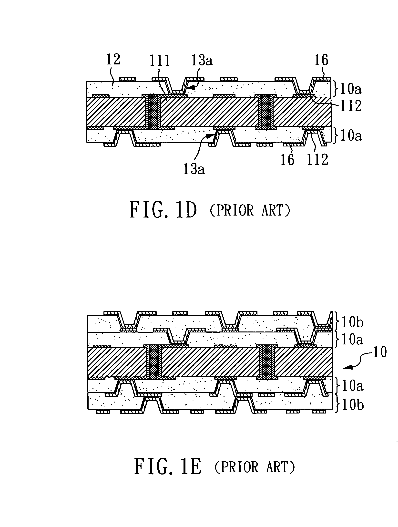
[0043]Please refer to FIGS. 3A to 3P to see the cross-section of another embodiment of the flip chip substrate structure of the present invention.

[0044]First, as shown in FIG. 3A, a carry board 301 is provided, which is a metal plate, preferably copper. Then, as shown in FIG. 3B, a first solder mask 302 is overlaid on the carry board 301, and plural first openings 303 are formed by exposure and development in the first solder mask 302, as shown in FIG. 3C.

[0045]A conductive metal layer 304, an etching-stop layer 305 and a metal layer 306 are formed orderly upward by electroplating or electroless plating in the first openings 303 of the first solder mask 302, which are depicted in FIGS. 3D to 3F, wherein the material of the conductive metal layer 304 and the metal layer 306 is copper, and the material of the etching-stop layer is gold because of its resistance to oxidation.

[0046]Subsequently, as shown in FIG. 3Q a dielectric layer 308 is formed on the surface of the metal layer 306 a...


PUM


Abstract

A flip chip substrate structure and a method to fabricate thereof are disclosed. The structure comprises a build up structure, a first solder mask and a second solder mask. Plural first and second electrical contact pads are formed on the first and second surface of the build up structure, respectively. A first solder mask having plural openings is formed on the first surface of the build up structure, and the openings expose the first electrical contact pads, wherein the aperture of the openings of the first solder mask are equal to the outer diameter of the first electrical contact pads. A second solder mask having plural openings is formed on the second surface of the build up structure, and the openings expose the second electrical contact pads, wherein the aperture of the openings of the second solder mask are smaller than the outer diameter of the second electrical contact pads.

Description

BACKGROUND OF THE INVENTION[0001]1. Field of the Invention[0002]The present invention relates to a flip chip structure, the method to manufacture the same and, more particularly, to a flip chip substrate structure that applies to non-through hole structures and improves circuit integration, and a method to manufacture flip chip substrates with a streamlined process.[0003]2. Description of Related Art[0004]With the development of the IT industry, the research in the industry is gradually turning to multifunctional and high performance electronic products. To meet the demands for high integration and miniaturization of semiconductor packaging, the circuit boards providing circuit connections among active and passive components are evolving from double layer boards to multi-layer boards in order to expand available layout areas on circuit boards within limited spaces by interlayer connection techniques, so as to accommodate the requirement of high circuit layout density of integrated c...

Claims


Application Information

Patent Timeline
IPC IPC(8): H05K1/11H01R12/04
CPCH01L21/4857H01L21/68H01L2924/0002H01L23/49822H05K3/205H05K3/243H05K3/28H05K3/4007H05K3/4682H05K2201/0367H05K2201/09481H05K2201/09563H05K2201/096H05K2201/099H05K2203/0384H01L2924/00
Inventor CHEN, BO-WEIWANG, HSIEN-SHOUHSU, SHIH-PING
Owner PHOENIX PRECISION TECH CORP
Why Eureka
Try Eureka