Wafer level chip scale packaging structure with low substrate resistance and manufacturing method thereof

A wafer-level chip and substrate resistance technology, used in semiconductor/solid-state device manufacturing, circuits, electrical components, etc., can solve problems such as wafer breakage, affecting chip performance, and inability to function, achieving low manufacturing costs and reducing Substrate resistance, easy operation effect

Active Publication Date: 2011-06-15
ALPHA & OMEGA SEMICON LTD
View PDF1 Cites 8 Cited by
  • Summary
  • Abstract
  • Description
  • Claims
  • Application Information

AI Technical Summary

Problems solved by technology

The wafer-level chip size package has the advantages of small size, light weight, good electrical conductivity, and simple process. However, the conductive column only solves the conductive problem in the vertical direction of the chip. For the electrical connection in the horizontal direction of the substrate, can't work
[0005] For double-diffused metal-oxide-semiconductor (DMOS), especially for wafer-level chip-scale packages with a common-drain dual-chip structure, such as figure 1 As shown, the conductive paths are shown by the arrows in Figu

Method used


Image

  • Wafer level chip scale packaging structure with low substrate resistance and manufacturing method thereof
  • Wafer level chip scale packaging structure with low substrate resistance and manufacturing method thereof
  • Wafer level chip scale packaging structure with low substrate resistance and manufacturing method thereof

Examples


Example Embodiment

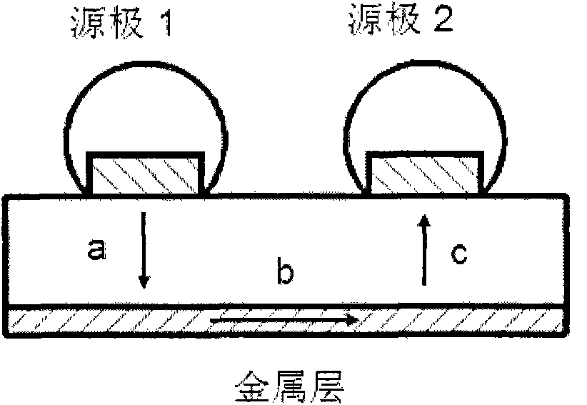
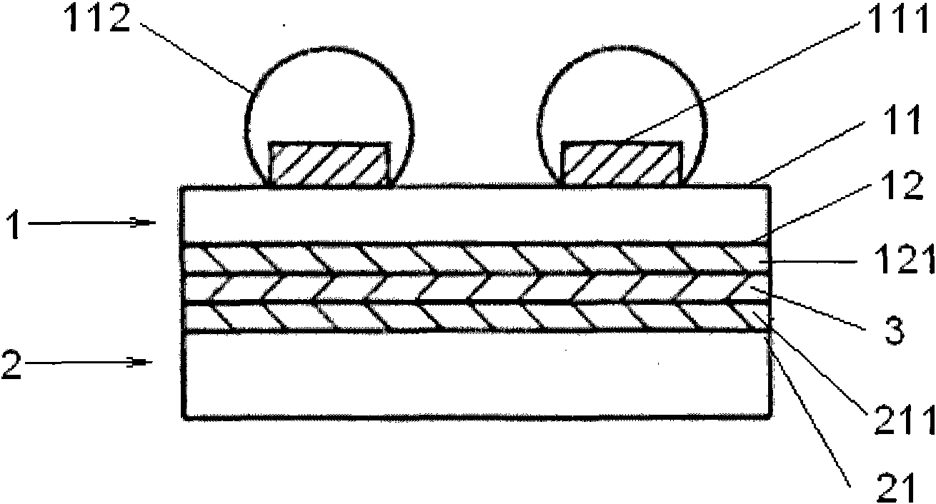
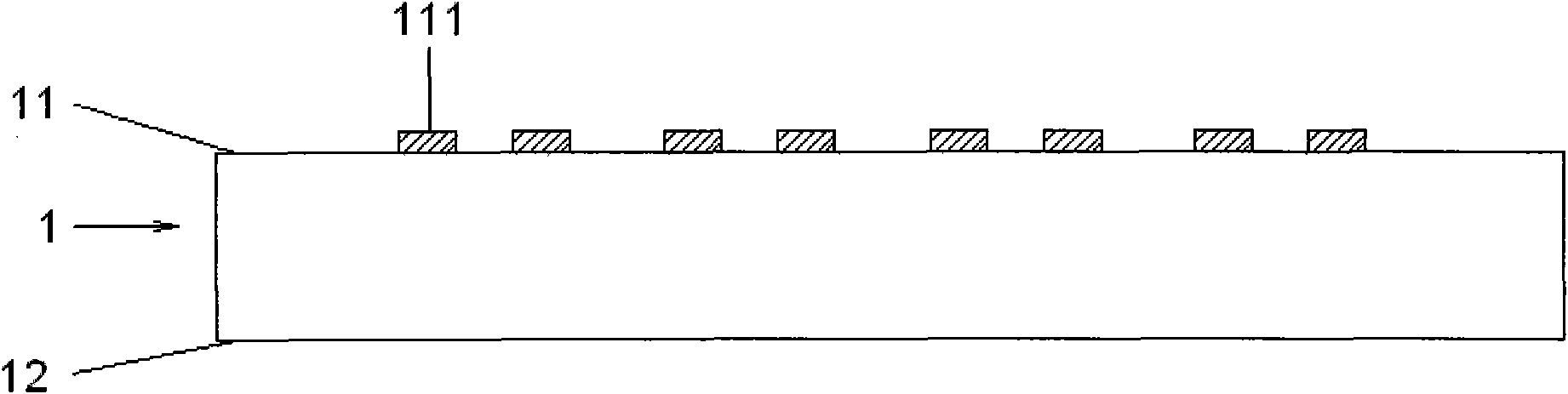
[0061] Example 1, please refer to the attached figure 2 As shown, a wafer-level chip size package with low substrate resistance includes a semiconductor chip 1 and a conductive reinforcement 2. The semiconductor chip 1 includes a semiconductor chip upper surface 11 and a semiconductor chip lower surface 12. On the semiconductor chip The surface 11 is provided with a plurality of integrated circuit chips (not shown in the figure), a plurality of UBM layers 111 and a plurality of solder balls 112 for chip connection on each UBM layer 111, The lower surface 12 of the semiconductor wafer is provided with a second metal layer 121; the conductive reinforcement 2 includes an upper surface 21 of the conductive reinforcement, and the upper surface 21 of the conductive reinforcement is provided with a first metal layer 211; the first metal layer 211 and the second metal A conductive epoxy resin 3 is provided between the layers 121 , and the first metal 211 and the second metal 121 are ...

Example Embodiment

[0063] Example 2, please refer to the attached Figure 11 As shown, a wafer-level chip-scale package with low substrate resistance includes a semiconductor chip 1' and a conductive reinforcement 2', and the semiconductor chip 1' includes a semiconductor chip upper surface 11' and a semiconductor chip lower surface 12 ', the upper surface 11' of the semiconductor wafer is provided with a plurality of integrated circuit chips (not shown in the figure), a plurality of under-bump metallization layers 111' and a chip for chip on each under-bump metallization layer 111' A plurality of solder balls 112' connected, the lower surface 12' of the semiconductor wafer is provided with a second metal layer 121'; the conductive reinforcement 2' includes an upper surface 21' of a conductive reinforcement, and the upper surface 21' of the conductive reinforcement is provided with a first The metal layer 211'; the first metal layer 211' is glued together with the second, so that the semiconduct...

Example Embodiment

[0065] Embodiment 3. In this embodiment, the structure of the wafer-level chip size package with low substrate resistance is the same as that of Embodiment 1, and the process is basically the same. The difference is that the first metal layer and the The second metal layer is two mutually fusible metals, so there is no need for the connection of solder. At high temperature, the two metals can be fused together, so that the conductive reinforcement and the semiconductor chip are combined together, with low The substrate lateral resistance. Preferably, the two mutually fusible metals are Au and Sn, respectively.


PUM

PropertyMeasurementUnit
Thicknessaaaaaaaaaa

Abstract

The invention discloses a wafer level chip scale packaging structure with low substrate resistance. The packaging structure comprises a semiconductor chip and a conducting reinforcing member, wherein the semiconductor chip comprises a semiconductor chip upper surface and a semiconductor chip lower surface; the semiconductor chip upper surface is provided with a plurality of integrated circuit chips, a plurality of under bump metallization (UBM) and a plurality of welding balls which are arranged on the UBM and are used for chip connection; the conducting reinforcing member comprises a conducting reinforcing member upper surface; the conducting reinforcing member upper surface is provided with a first metal layer; and the first metal layer of the conducting reinforcing member and the semiconductor chip lower surface are bonded together in the manufacturing process. The wafer level chip scale packaging structure and the manufacturing method have the beneficial effects of improving the chip substrate conductivity and reducing the substrate resistance and the transverse on-resistance on the one hand, and improving the reliability of the chip while reducing the package scale and ensuring the wafer and the chip not to be easily damaged in the process operation on the other hand.

Description

technical field [0001] The invention relates to a semiconductor packaging structure and a manufacturing method, in particular to a wafer-level chip size packaging with low substrate resistance and a manufacturing method thereof. Background technique [0002] Wafer Level Chip Scale Packaging (WLCSP) is an integrated circuit chip packaging technology, which is different from the traditional chip packaging method (cutting first, then packaging and testing, and at least 20% of the volume of the original chip after packaging) , this latest technology is to carry out packaging and testing on the wafer first, and then cut into IC particles one by one, so the volume after packaging is equal to the original size of the IC die. For wafer-level chip packaging, the packaging area is the same as The chip area ratio is less than 1.2. [0003] Recently developed electronic devices such as mobile phones, laptop computers, video cameras, personal digital assistants, and other similar device...

Claims


Application Information

Patent Timeline
IPC IPC(8): H01L23/48H01L23/482H01L23/488H01L21/60
CPCH01L2224/73253
Inventor 冯涛
Owner ALPHA & OMEGA SEMICON LTD
Why Eureka
Try Eureka