Charged particle beam apparatus

a particle beam and apparatus technology, applied in the direction of material analysis using wave/particle radiation, instruments, nuclear engineering, etc., can solve the problems of affecting the effect of aberration correction, complicated readjustment, and method limitations, and achieve the effect of reducing the influence of nois

Inactive Publication Date: 2008-03-20
HITACHI HIGH-TECH CORP
View PDF13 Cites 13 Cited by
  • Summary
  • Abstract
  • Description
  • Claims
  • Application Information

AI Technical Summary

Benefits of technology

[0022]According to this invention, the stable charged particle beam apparatus to enable high-resolution observation by reducing the influence by the noise of a large number of power supplies used in the aberration corrector can be realized.

Problems solved by technology

Ripple noise of a voltage impressed to an electrode causes a beam to be deviated laterally at random, enlarging its spot size, which impairs an effect of aberration correction.
Since these current and voltage are restricted by a maximum voltage and a maximum current that can be impressed by control power supplies of the aberration corrector, this method has limitations.
Moreover, this technique needs to newly reset reference fundamental rays when the overall magnification is varied according to the influence of the power supply noise, which needs complicated readjustment each time.

Method used


Image

  • Charged particle beam apparatus
  • Charged particle beam apparatus
  • Charged particle beam apparatus

Examples


first embodiment

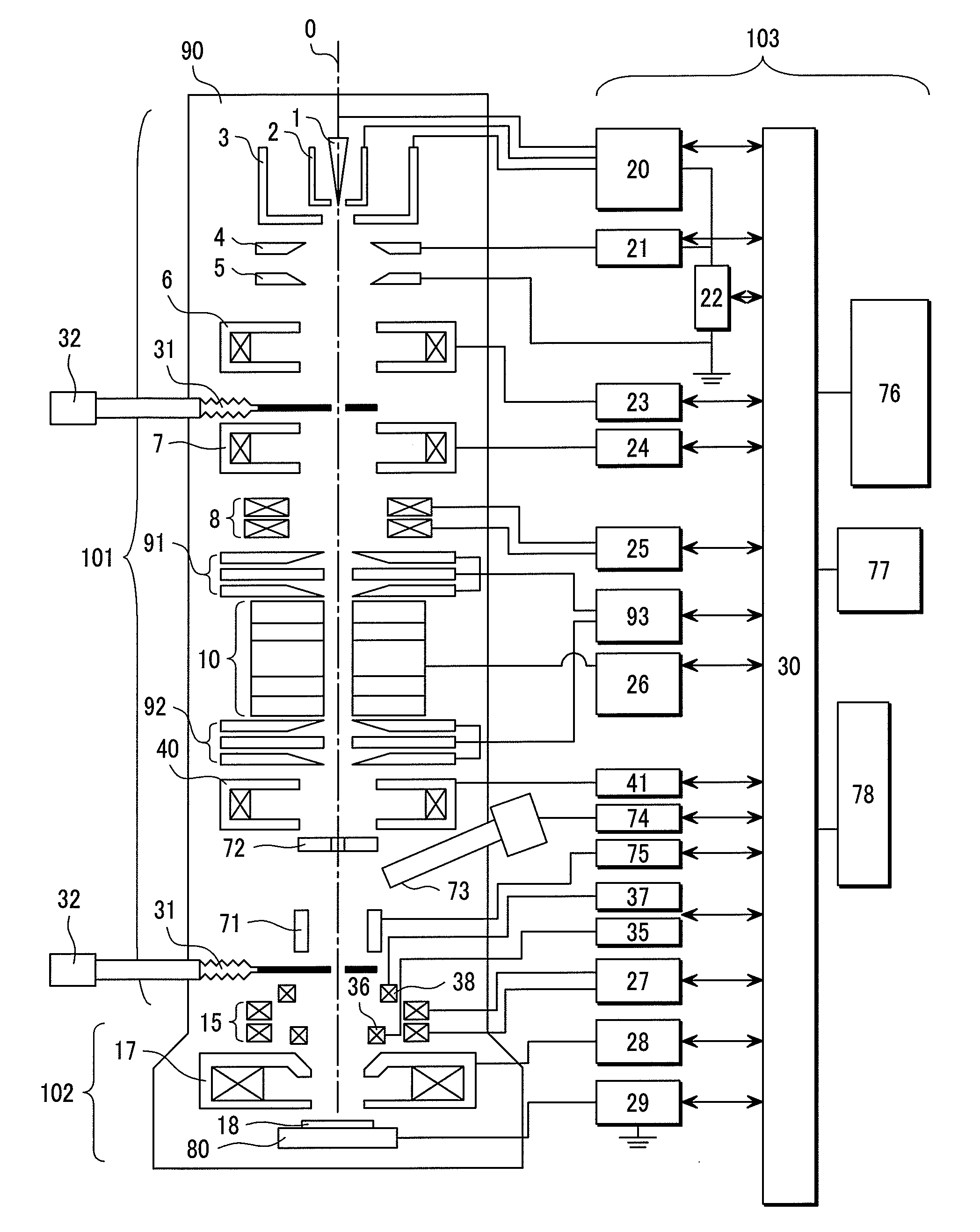
[0030]FIG. 1 shows an outline configuration of a scanning electron microscope as a first embodiment according to this invention. The scanning electron microscope of this embodiment as a whole is constructed with an SEM column 101 that is inside a vacuum chamber 90 and houses an irradiation optics for irradiating an electron beam (primary charged particle beam) onto a specimen or making the electron beam scan it, a specimen chamber 102 for housing a specimen stage, a control unit 103 for controlling component parts of the SEM column 101, the specimen chamber 102, and the like. The control unit 103 has further connections to a data storage 76 for storing predetermined information, a monitor 77 for displaying an acquired image, and an operation console 78 for serving as a man-machine interface between the apparatus and an apparatus user. The console is constructed, for example, with information input means, such as a keyboard and a mouse.

[0031]First, constituents inside the SEM column ...

second embodiment

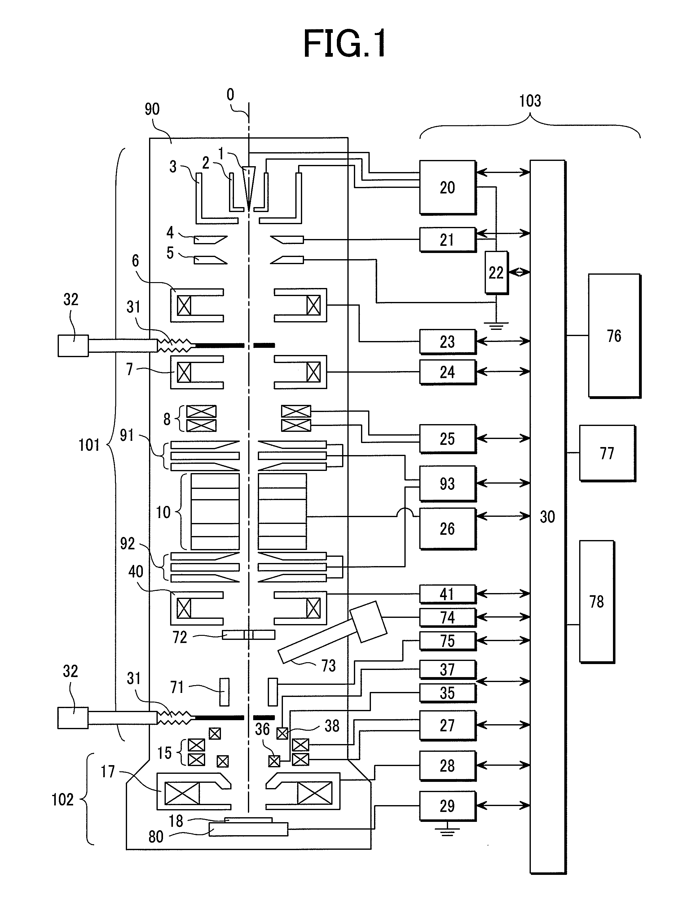
[0040]In this embodiment, the case of the critical-dimension-measurement SEM (Scanning Electron Microscope) will be described. As the specimen whose length is measured, there can be enumerated a semiconductor wafer on which a circuit pattern is formed, a chip, or a piece of the specimen that is prepared by cutting a portion from the wafer, etc.

[0041]FIG. 2 shows a hardware configuration of the critical-dimension-measurement SEM as a second embodiment according to this invention. That a whole configuration of the critical-dimension-measurement SEM is constructed with the SEM column 101, the specimen chamber 102 for housing a specimen stage, the control unit 103, etc. is the same as the charged particle beam application apparatus explained in the first embodiment, but it has a preparation chamber (load chamber) 60 for introducing a specimen whose length is measured into the apparatus. The preparation chamber 60 and the specimen chamber 102 of a body of the apparatus are partitioned by...

third embodiment

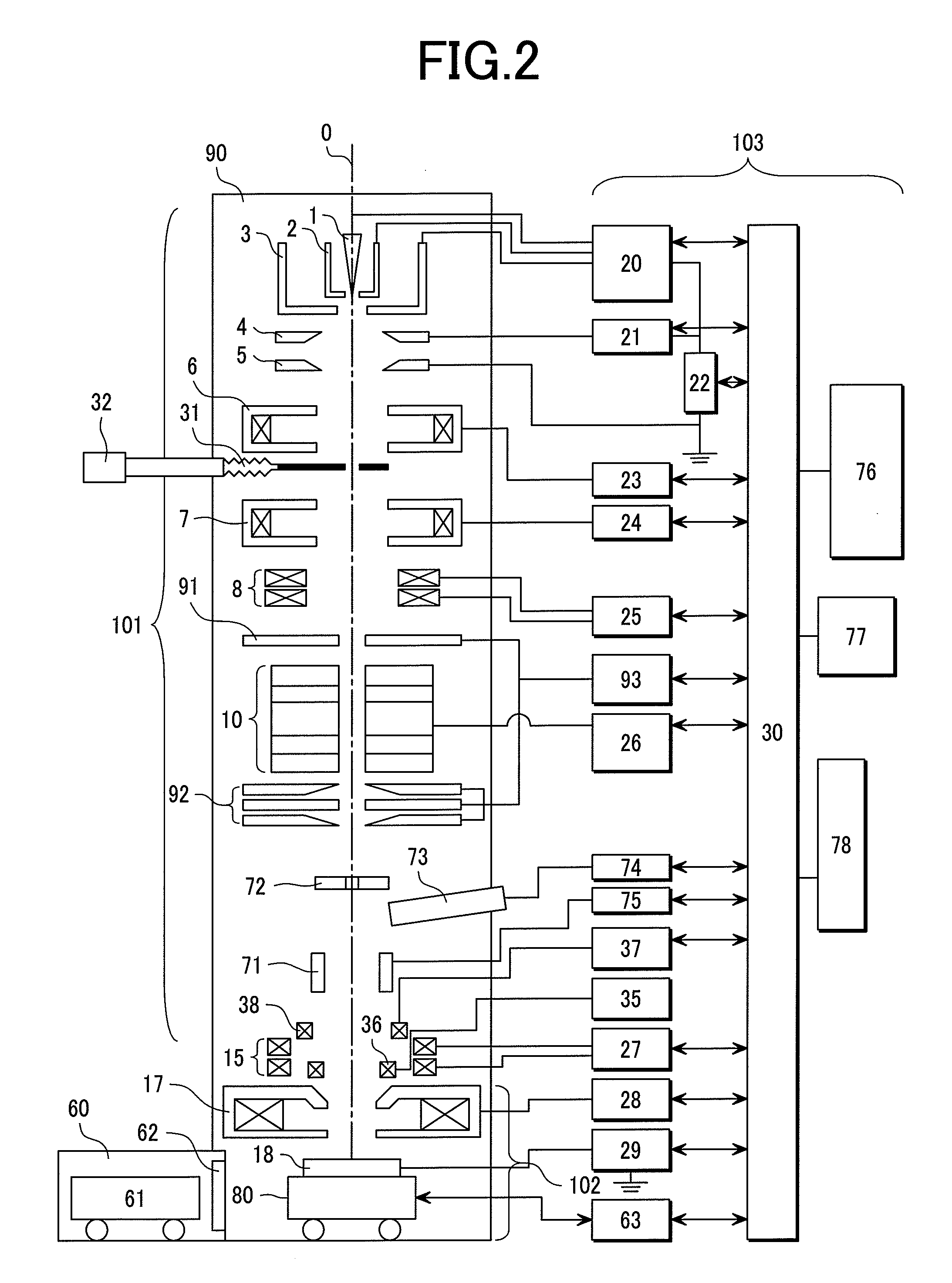
[0045]FIG. 3 shows one configuration example of the aberration corrector used in this invention. In this embodiment, a configuration example of four stages of dodecapoles will be explained.

[0046]The aberration corrector 10 is configured such that, in a casing 120 made of nonmagnetic metal, the pre-stage accelerating electrode (upper electrode) 93 and a post stage accelerating electrode (lower electrode) 94 are provided along the optical axis through insulator material 119 and an acceleration voltage is impressed to the electrodes 93, 94 via a voltage feedthrough 121 from the vacuum outside. Between the pre- and post stage accelerating electrodes 93, 94, four stages of dodecapoles 111, 112, 113, and 114 are being fixed to the casing 120 through insulators 123, 124. The electrostatic dodecapoles 111, 114 are made of nonmagnetic metal, and a voltage is impressed to them via the voltage feedthroughs 121 from the vacuum outside. The electro-magnetic dodecapoles 112, 113 are made of soft ...


PUM


Abstract

The present invention provides a stable charged particle beam apparatus to enable high-resolution observation by reducing the influence of the noise of a large number of power supplies used in an aberration corrector. The charged particle beam apparatus that has: an SEM column for irradiating an electron beam onto a specimen and making the electron beam scan it; a specimen chamber for housing a specimen stage on which the specimen is placed and held; a detector for detecting secondary electrons generated by the scanning of the electron beam; display means for displaying an output signal of the detector as an SEM image; and a control unit for controlling component parts including the SEM column, the specimen chamber, and the display means. The SEM column has a pair of accelerating electrodes and an aberration corrector that is placed between the pair of accelerating electrodes and corrects aberration of the electron beam, and accelerates the electron beam during a period when being transmitted through the aberration corrector by a high voltage being impressed across the pair of accelerating electrodes.

Description

CLAIM OF PRIORITY[0001]The present invention claims priority from Japanese application JP 2006-169787 filed on Jun. 20, 2006, the content of which is hereby incorporated by reference on to this application.BACKGROUND OF THE INVENTION[0002]This invention relates to charged particle beam application technologies, and more specifically, to charged particle beam apparatuses, such as a scanning electron microscope (SEM) equipped with an aberration corrector, an electron beam semiconductor inspection system, a critical dimension measurement SEM, and a focused ion beam apparatus.[0003]Since the scanning electron microscope can observe the surface of an object with resolution higher than that of the optical microscope, it is widely used not only as apparatuses for material research but also as industrial apparatuses, such as for dimension measurement of a pattern on a semiconductor wafer that is being advanced in miniaturization in recent years and inspection of surface foreign matters. In ...

Claims


Application Information

Patent Timeline
Patent Type & Authority Applications(United States)
IPC IPC(8): G21K7/00
CPCH01J37/153H01J37/248H01J2237/1534H01J2237/04735H01J37/28
Inventor KAWASAKI, TAKESHISATO, MITSUGUEZUMI, MAKOTONAKANO, TOMONORI
Owner HITACHI HIGH-TECH CORP
Why Eureka
Try Eureka