Field-effect transistor and method of manufacturing the same

a field-effect transistor and field-effect technology, applied in the field of field-effect transistors, can solve the problems of deterioration of transistor characteristics, less moisture resistance of laminated insulating films, and increased cost of airtight packages, so as to reduce the cost of manufacturing processes

Active Publication Date: 2008-04-17
MITSUBISHI ELECTRIC CORP
View PDF5 Cites 31 Cited by
  • Summary
  • Abstract
  • Description
  • Claims
  • Application Information

AI Technical Summary

Benefits of technology

[0011]Accordingly, an object of the present invention is to provide a low-cost field-effect transistor with moisture-resistant treatment being effected around a gate by laminating a thick moisture-resistant insulating film which suppresses increase in gate capacitance, and a method of manufacturing the field-effect transistor
[0013]An effect of the field-effect transistor according to the present invention is that, a cavity can be formed between a portion of the gate electrode corresponding to a canopy of an open umbrella and the semiconductor layer by depositing a thick silicon nitride film having the effect of resisting moisture by catalytic CVD, so process steps of forming the cavity can be eliminated, and thus cost in the manufacturing process can be reduced.

Problems solved by technology

However, with regard to a compound semiconductor field-effect transistor used in a transmission / reception module of a terminal, in addition to basically very low moisture resistance of the compound semiconductor itself, the moisture resistance of a laminated insulating film is not so high.
When the film thickness is as small as 100 nm or less, because the covering is not sufficient at irregularities and for other reasons, moisture can easily intrudes, which deteriorates characteristics of the transistor.
However, because such an airtight package is more expensive than a transistor chip itself, it is required to enhance the moisture resistance of the transistor chip itself in order to reduce costs while adopting a simpler package.
However, because the transistor operates in a high frequency band, if the moisture-resistant insulating film is made thicker, the spatial capacity increases, which results in deteriorated characteristics.
In particular, in an HEMT structure which is often used in a millimeter wave band, existence of an insulating film between a gate and a semiconductor surface results in considerable increase in gate capacitance and considerable reduction in gain.

Method used


Image

  • Field-effect transistor and method of manufacturing the same
  • Field-effect transistor and method of manufacturing the same
  • Field-effect transistor and method of manufacturing the same

Examples


embodiment 1

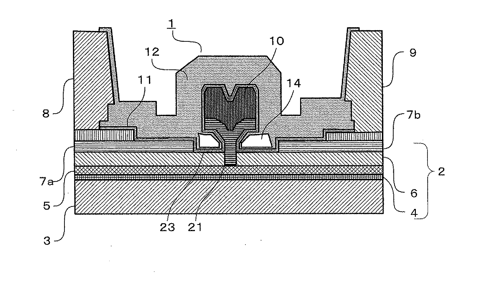
[0022]FIG. 1 is a sectional view of a field-effect transistor according to Embodiment 1 of the present invention.

[0023]As illustrated in FIG. 1, a field-effect transistor 1 according to Embodiment 1 of the present invention has a buffer layer 3 formed of an undoped GaAs epitaxial layer grown on a semi-insulating GaAs substrate as a semi-insulating substrate, a channel layer 4 formed of an undoped GaAs epitaxial layer grown on the buffer layer 3, a gate contact layer 5 formed of an undoped AlGaAs epitaxial layer grown on the channel layer 4, a gate embedding layer 6 formed of an undoped GaAs epitaxial layer grown on the gate contact layer 5, and two capping layers 7a and 7b formed of an n+-type GaAs epitaxial layer grown on the gate embedding layer 6 and patterned so as to be apart from each other by a predetermined distance. It is to be noted that the buffer layer 3, the channel layer 4, the gate contact layer 5, the gate embedding layer 6, and the capping layers 7a and 7b are compr...

embodiment 2

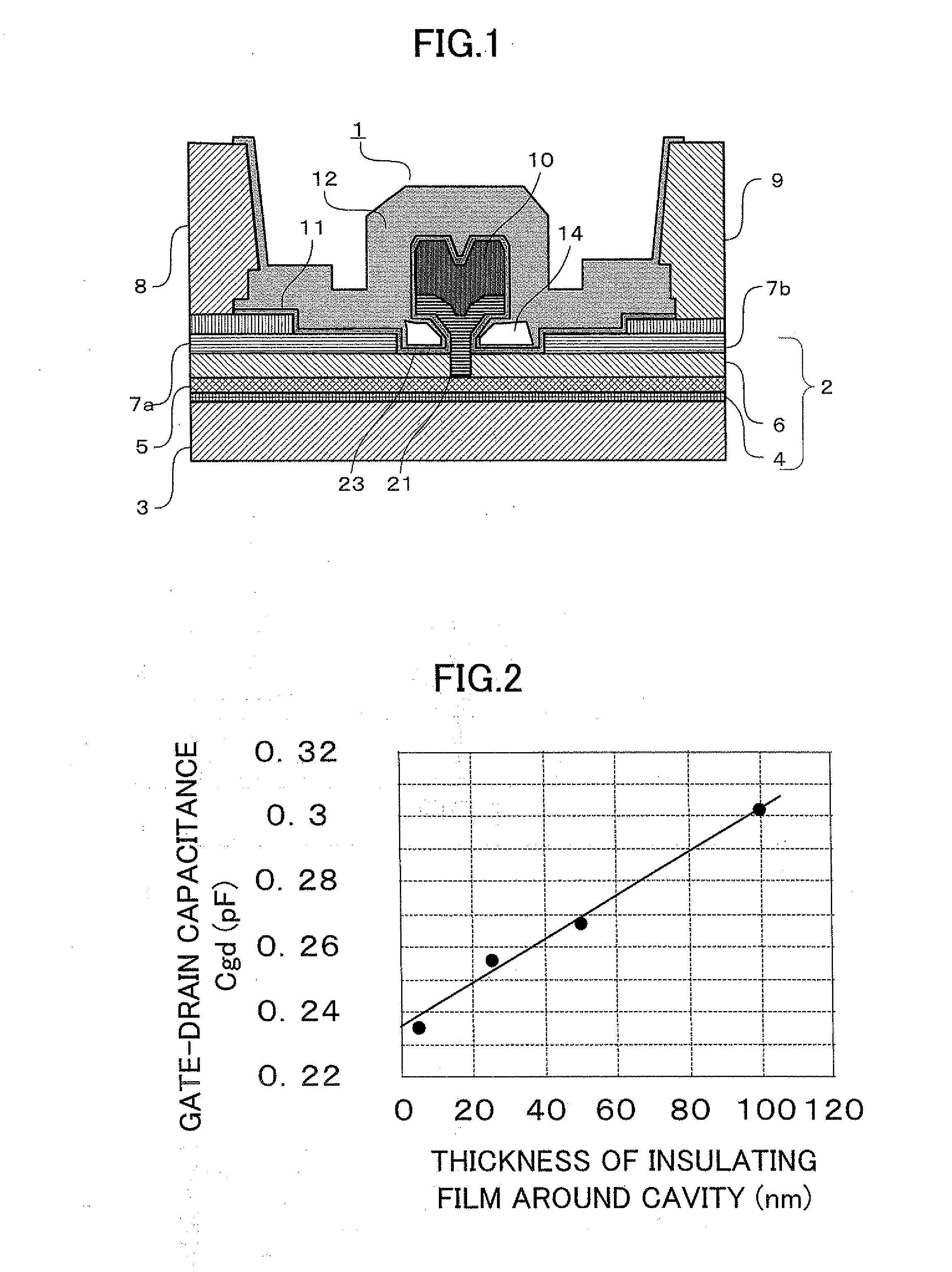
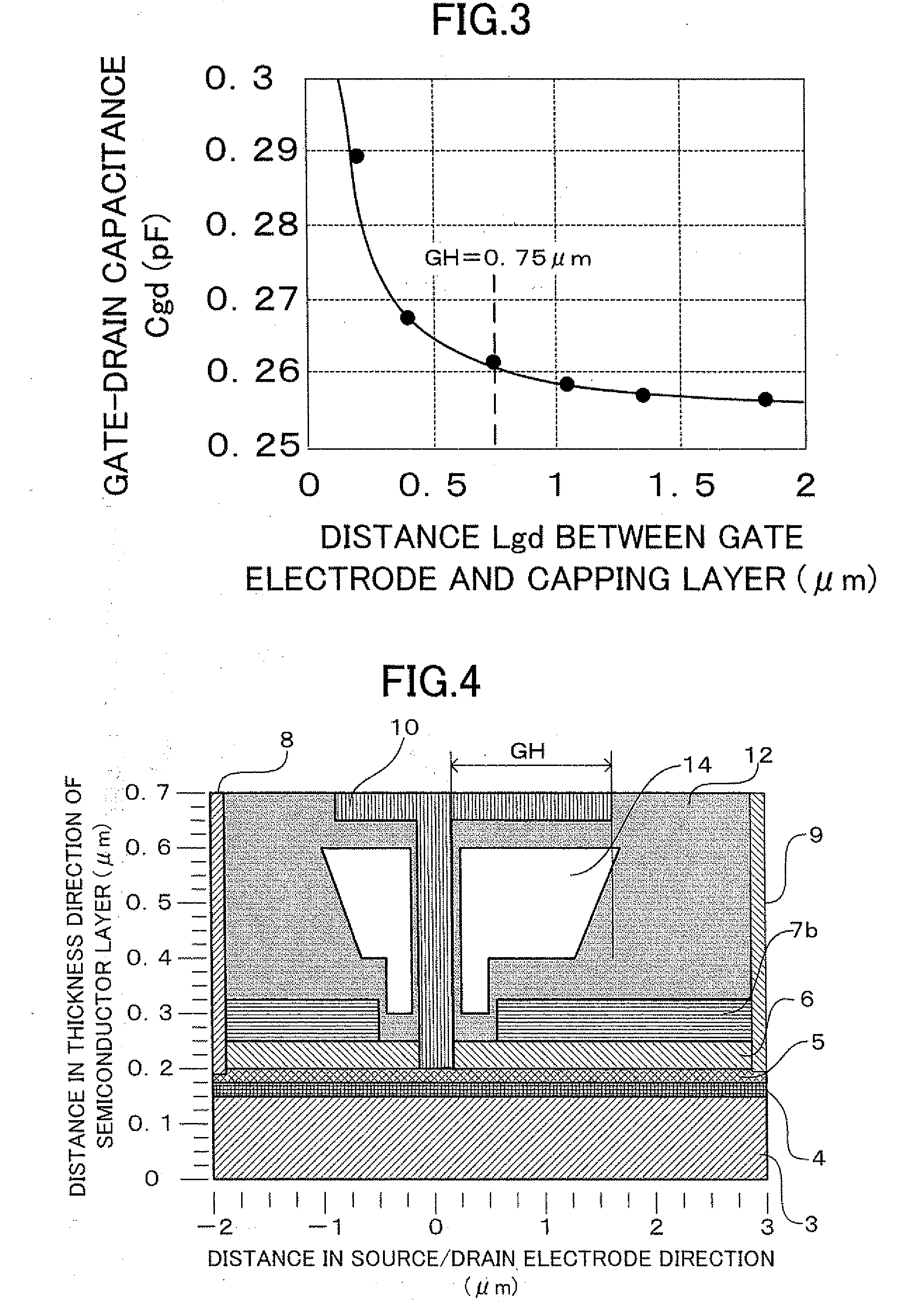
[0046]FIG. 4 illustrates a computing device model used when the gate-drain capacitance is simulated.

[0047]In Embodiment 2, the length by which the portion of the gate electrode 10 corresponding to the canopy of the open umbrella of the field-effect transistor 1 according to Embodiment 1 overhangs on the side of the drain electrode 9 (hereinafter referred to as “gate overhang on drain side GH”) is made varied to simulate the gate-drain capacitance Cgd.

[0048]In the simulation, the computing device model illustrated in FIG. 4 is used, and SiNx having the relative permittivity of 7.55 fills the space on the gate and between the source electrode 8 and the drain electrode 9. The gate-drain capacitance Cgd is simulated with regard to a structure where the cavity 14 is formed between the portion of the gate electrode 10 corresponding to the canopy of the open umbrella and the semiconductor layer 2 (structure according to Embodiment 2), a structure where a low permittivity film having the re...

embodiment 3

[0055]FIG. 6 is a sectional view of a field-effect transistor according to Embodiment 3 of the present invention.

[0056]A field-effect transistor 1B according to Embodiment 3 of the present invention is similar to the field-effect transistor 1 according to Embodiment 1 except for the gate electrode 10B, and thus, like reference symbols are used to denote like or identical members and description of those is omitted.

[0057]As illustrated in FIG. 6, the gate electrode 10B according to Embodiment 3 has a Γ-shaped gate structure where a portion corresponding to a canopy of an open umbrella overhangs only on the side of the drain electrode 9. SiNx fills the space between the portion of the gate electrode 10B corresponding to the canopy of the open umbrella and the semiconductor layer 2, from the side surface of the gate electrode 10B corresponding to a shank of the umbrella so as to extend to the side of the drain electrode 9, and the remaining space is left as the cavity 14.

[0058]Withstan...


PUM


Abstract

A low-cost field-effect transistor with a moisture-resistant gate covered by a thick moisture-resistant insulating film which suppresses an increase in gate capacitance, and a method of manufacturing the field-effect transistor. The field-effect transistor, has one of a T-shaped gate electrode and Γ-shaped gate electrode, a drain electrode, and a source electrode, the source electrode and the drain electrode being electrically connected through an n-doped semiconductor region. The gate, source, and drain electrodes are located on a semiconductor layer which includes an insulating film having a thickness of 50 nm or less and covering a surface of the gate electrode and a surface of the semiconductor layer. A silicon nitride film, deposited by catalytic CVD, covers the insulating film and includes a void volume located between a portion of the gate electrode corresponding to a canopy of an open umbrella and the semiconductor layer.

Description

BACKGROUND OF THE INVENTION[0001]1. Field of the Invention[0002]The present invention relates to a field-effect transistor, which is mainly suitable for use in a high frequency band such as equal to or higher than 1 GHz, and to a method of manufacturing the same.[0003]2. Description of the Related Art[0004]Various kinds of systems based on WiMAX or the like, for radio communication using a high frequency band such as equal to or higher than 1 GHz, including mobile phones which are prevailing these days, are under development and infrustructing. Further, markets for millimeter wave radio systems such as 60-GHz band high-speed and large-capacity communication systems and 70-to-80-GHz band vehicle-mounted radar systems are expected to expand in the future. A compound semiconductor, in particular, a field-effect transistor such as a MESFET, an HFET, or an HEMT in which a GaAs is used as a substrate is used for parts for transmitting / receiving a radio signal in such a high frequency band...

Claims


Application Information

Patent Timeline
Patent Type & Authority Applications(United States)
IPC IPC(8): H01L29/739H01L21/337
CPCH01L29/7787H01L29/0649H01L29/80
Inventor AMASUGA, HIROTAKATOTSUKA, MASAHIRO
Owner MITSUBISHI ELECTRIC CORP
Why Eureka
Try Eureka