Solid-state imaging device, imaging apparatus and camera

a technology of solid-state imaging and imaging apparatus, which is applied in the scanning details of color television, television systems, and television systems, etc., can solve the problems of two pixels, difficult to secure the area of a photoelectric conversion unit sufficiently, and restricted control of each transistor, so as to achieve high sensitivity, enhance optical properties, and maintain resolution

Inactive Publication Date: 2008-04-17
SONY CORP
View PDF6 Cites 64 Cited by
  • Summary
  • Abstract
  • Description
  • Claims
  • Application Information

AI Technical Summary

Benefits of technology

[0060]According to the solid-state imaging device according to an embodiment of the present invention, there is an advantage wherein the light receiving area of the photoelectric conversion unit of each pixel is sufficiently secured, so high sensitivity can be realized while maintaining resolution, thereby enhancing optical property. Also, an arrangement is employed wherein a pixel transistor is shared with four pixels, whereby wiring can be simplified, and an effective pixel layout can be provided.
[0061]According to the imaging apparatus according to an embodiment of the present invention, the solid-state imaging device is employed, whereby the same advantages as those described above can be obtained, and also an advantage can be obtained wherein pixel property, e.g., high sensitivity can be realized.
[0062]According to an embodiment of the present invention, an imaging apparatus and a camera can be provided wherein the driving load of a pixel circuit is reduced.
[0063]According to an embodiment of the present invention, the area usage efficiency of a semiconductor board can be raised, and the occupied size of a transistor region can be increased.

Problems solved by technology

A problem regarding which the need to solve has been recognized, is in that with a so-called honeycomb pixel array, a charge-to-voltage conversion unit is disposed at a side portion of a pixel, which excels in readout property, but includes a problem in that the condensing spot area is compressed, and also, in that even if the shared portion of a charge-to-voltage conversion unit (e.g., floating diffusion: FD) which is a charge-to-voltage conversion unit is disposed between pixels, sharing a pixel transistor between the two pixels makes it difficult to sufficiently secure the area of a photoelectric conversion unit (e.g., photodiode: PD).
Also, with a solution proposed by sharing a transistor of a pixel circuit, a problem has been known in that there are many cases wherein control of each transistor is restricted.

Method used


Image

  • Solid-state imaging device, imaging apparatus and camera
  • Solid-state imaging device, imaging apparatus and camera
  • Solid-state imaging device, imaging apparatus and camera

Examples


third embodiment

[0111]A third embodiment of the present invention will be described below with reference to the drawings. FIG. 8 is a block diagram illustrating one configuration example of principal units of an imaging apparatus according to a third embodiment of the present invention.

[0112]The imaging apparatus 2001 includes a pixel circuit 2010, a pixel array unit 2011, a horizontal scan circuit (HSCN) 2012, an amplifier 2121, a vertical scan circuit (VSCN) 2013, a signal processing circuit 2014, an analog-to-digital converter (A / D) 2015, a timing adjusting unit 2016, a timing generator (TG) 2017, and a lens 2018.

[0113]With the pixel array unit 2011, for example, the pixel circuit 2010 is arrayed with a predetermined array mode in a matrix shape.

[0114]Also, with the pixel array unit 2011, the vertical scan circuit 2013 and each row of a pixel array are connected with a reset line RSTL, a transfer selection line TRFL, and a selection line SELL, and each column of the pixel array is arrayed with a...

fourth embodiment

[0170]Description will be made below regarding a layout example of a pixel circuit according to a fourth embodiment of the present invention. FIGS. 13A and 13B are diagrams illustrating one layout example of a pixel circuit according to the fourth embodiment of the present invention.

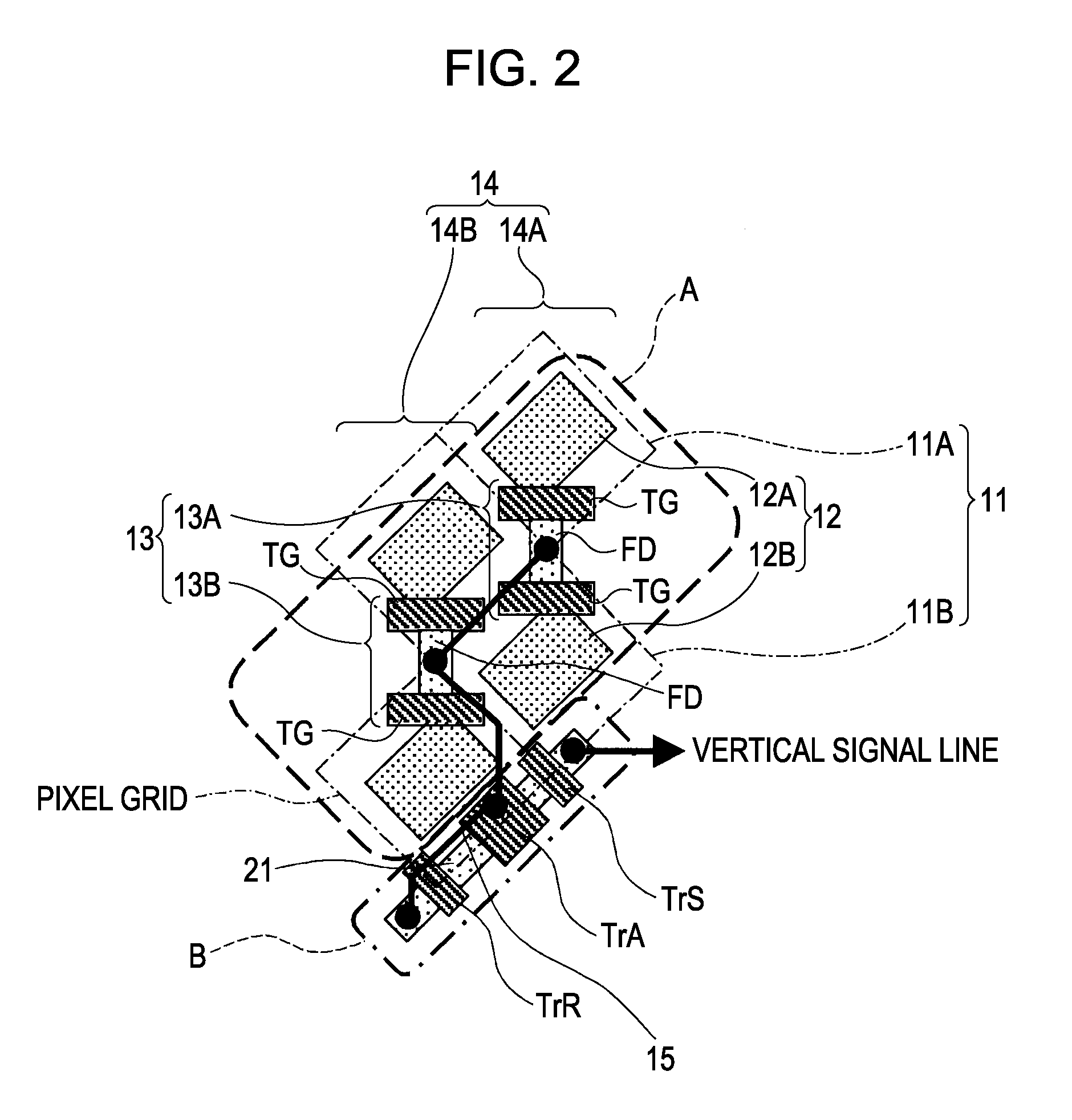
[0171]The pixel group GRP 2002 shown in FIG. 13A is one example wherein the two pixel circuits shown in FIG. 9A share the source diffusion layer 2210a of the amplification transistor, and the two pixel circuits 2002a are disposed in a diagonal direction as to the source diffusion layer 2210a of the amplification transistor. FIG. 13B is an equivalent circuit diagram of the pixel group GRP 2002 shown in FIG. 13A.

[0172]The pixel group GRP 2002 shown in FIG. 13B is one example wherein the two unit equivalent circuits 2002b shown in FIG. 13B share the signal output terminal 2211b, and are disposed in a diagonal direction as to the signal output terminal 2211b.

[0173]FIG. 14 is a diagram wherein the pixel grou...

fifth embodiment

[0219]The fifth embodiment of the present invention will be described below with reference to the drawings. FIG. 16 is a block diagram illustrating one configuration example of principal units of an imaging apparatus according to the fifth embodiment of the present invention.

[0220]The present imaging apparatus 2001a includes a pixel circuit 2010, a pixel array unit 2011, a horizontal scan circuit (HSCN) 2012a, an amplifier 2121, a vertical scan circuit (VSCN) 2013, a signal processing circuit 2014, an analog-to-digital converter (A / D) 2015, a timing adjusting unit 2016a, a timing generator TG (2017), and a lens 2018.

[0221]The timing adjusting unit 2016a is disposed in the inside of the horizontal scan circuit 2012a, delays an analog signal input from the pixel array unit 2011 via the amplifier 2121 by a predetermined time in accordance with a predetermined procedure, and outputs this to the signal processing circuit 2014. Description will be made later regarding the operation of the...


PUM


Abstract

A solid-state imaging device includes: multiple pixels making up a slanted grid array inclined to a scanning direction, which include a photoelectric conversion unit configured to convert incident light quantity into an electric signal; and a charge-to-voltage conversion unit configured to convert signal charge read out from the photoelectric conversion unit disposed between two pixels adjacent to each other in the diagonal direction of the pixels of the multiple pixels into voltage; wherein the charge-to-voltage conversion unit is shared with the two pixels; and wherein a set of transistor group are disposed in a sharing block, which is configured of a pixel pair made up of the two pixels adjacent to each other in the diagonal direction, and a pixel pair adjacent to that pixel pair, including wiring to which the charge-to-voltage conversion unit of each pixel pair is connected.

Description

CROSS REFERENCES TO RELATED APPLICATIONS[0001]The present invention contains subject matter related to Japanese Patent Application JP 2006-279733 filed in the Japanese Patent Office on Oct. 13, 2006, Japanese Patent Application JP 2006-306278 filed in the Japanese Patent Office on Nov. 13, 2006, and Japanese Patent Application JP 2007-052935 filed in the Japanese Patent Office on Mar. 2, 2007, the entire contents of which are incorporated herein by reference.BACKGROUND OF THE INVENTION[0002]1. Field of the Invention[0003]The present invention relates to a solid-state imaging device and an imaging apparatus. Also, the present invention relates to an imaging apparatus and a camera, which include an imaging device such as a CCD (Charge Coupled Device), CMOS (Complementary Metal Oxide Semiconductor) sensors and so forth.[0004]2. Description of the Related Art[0005]As digital cameras have come into widespread use in recent years, high resolution has come to be demanded even of lower-pric...

Claims


Application Information

Patent Timeline
Patent Type & Authority Applications(United States)
IPC IPC(8): H04N5/225H04N5/335
CPCH01L27/14603H01L27/14609H01L27/14641H04N5/3741H04N5/3696H04N25/766H04N25/70H04N25/134H04N25/77H04N25/75
Inventor KUDOH, YOSHIHARU
Owner SONY CORP
Why Eureka
Try Eureka