Wireless Processor, Wireless Memory, Information System, And Semiconductor Device

a technology of information system and semiconductor device, applied in the direction of instruments, basic electric elements, electromagnetic radiation sensing, etc., can solve the problems of reducing the highest temperature of the process, poor heat resistance of plastic materials, etc., and achieves the effect of easy memory expansion, processing, and high valu

Inactive Publication Date: 2008-04-24
SEMICON ENERGY LAB CO LTD
View PDF34 Cites 101 Cited by
  • Summary
  • Abstract
  • Description
  • Claims
  • Application Information

AI Technical Summary

Benefits of technology

[0028]According to the invention, a processor can be connected wirelessly. That is, data and power can be transmitted and received wirelessly between the processor and a semiconductor device. Therefore, a processor can be easily increased. In this manner, wireless transmission and reception of power or signals can add high value to a processor.
[0029]According to the invention, a memory can be connected wirelessly. That is, data and power can be transmitted and received wirelessly between a memory and a semiconductor device. Therefore, a memory can be easily increased. In this manner, wireless transmission and reception of power or signals can add high value to a memory and a semiconductor device.
[0030]According to the invention, a wireless processor or a wireless memory which is superior in shock resistance and flexibility can be obtained by forming a high functional integrated circuit such as an arithmetic unit on a plastic substrate.

Problems solved by technology

However, a plastic material is generally poor in heat resistance, thus the highest temperature of the process is required to be decreased.

Method used


Image

  • Wireless Processor, Wireless Memory, Information System, And Semiconductor Device
  • Wireless Processor, Wireless Memory, Information System, And Semiconductor Device
  • Wireless Processor, Wireless Memory, Information System, And Semiconductor Device

Examples


embodiment mode 1

[0059]In this embodiment mode, a configuration of a wireless processor of the invention is described.

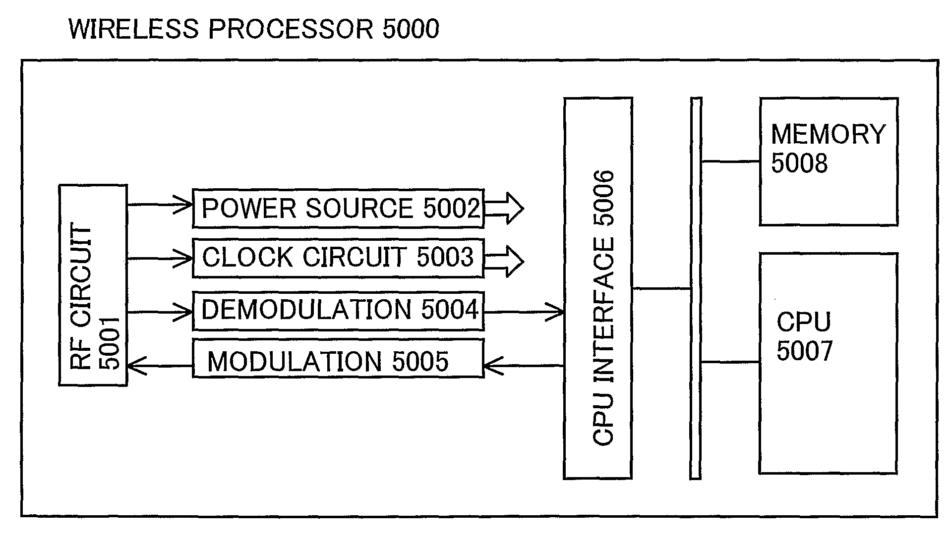
[0060]FIG. 1 shows a typical circuit configuration of a wireless processor. In FIG. 1, a wireless processor 5000 includes an RF circuit 5001, a power source circuit 5002, a clock generating circuit 5003, a data demodulation circuit 5004, a load modulation circuit 5005, a CPU interface 5006, an arithmetic processing unit (hereinafter referred to as a CPU as a function as a so-called CPU is included) 5007, and a memory 5008.

[0061]The wireless processor 5000 can receive a power supply through electromagnetic waves and can also transmit and receive data through an antenna included in the RF circuit. The power may be supplied from an incorporated battery instead of being supplied through the antenna, or both of these may be used in combination. Furthermore, one of a light detecting element and a light emitting element may be incorporated as a data transmission / reception unit so that infra...

embodiment mode 2

[0072]In this embodiment mode, an example of a circuit configuration of a wireless processor interface 5200 is described with reference to FIG. 4.

[0073]The wireless processor interface 5200 shown in FIG. 4 is connected to a PCI bus and includes a PCI interface 5201, a control circuit 5202, and an electric wave interface 5203. The electric wave interface 5203 depends on a communication method such as an electromagnetic induction method and a microwave method.

[0074]The electric wave interface 5203 includes, for example, a data transmission path 5708, a data reception path 5709, an oscillation circuit 5701, and an antenna 5704. When transmission data is inputted to the data transmission path 5708 in such an electric wave interface 5203, a signal from the oscillation circuit 5701 is modulated in a modulation circuit 5702, amplified in an amplifier circuit 5703, and transmitted to the antenna 5704. On the other hand, when a reception signal from the antenna 5704 is inputted to the data r...

embodiment mode 3

[0077]According to the wireless processor of the invention, a plurality of wireless processors can be connected by one wireless processor interface. In this embodiment mode, an example of such a mode is described with reference to FIG. 6.

[0078]FIG. 6 shows a system including a plurality of wireless processors 5303 to 5305 and a semiconductor device 5301 which includes a wireless processor interface 5302.

[0079]Description is made on a configuration in which the wireless processor interface 5302 recognizes and controls the plurality of wireless processors. First, the case where each of the wireless processors has a unique ID number is described, and then the case where the wireless processors are each identical and do not have unique ID numbers is described. In either case, each of the wireless processors has an ID number which is recognizable in the system when the wireless processor is incorporated in the system. Reading the ID number, the system can selectively communicate with the...


PUM


Abstract

The invention provides a processor obtained by forming a high functional integrated circuit using a polycrystalline semiconductor over a substrate which is sensitive to heat, such as a plastic substrate or a plastic film substrate. Moreover, the invention provides a wireless processor, a wireless memory, and an information processing system thereof which transmit and receive power or signals wirelessly. According to the invention, an information processing system includes an element forming region including a transistor which has at least a channel forming region formed of a semiconductor film separated into islands with a thickness of 10 to 200 nm, and an antenna. The transistor is fixed on a flexible substrate. The wireless processor in which a high functional integrated circuit including the element forming region is formed and the semiconductor device transmit and receive data through the antenna.

Description

TECHNICAL FIELD[0001]The present invention relates to a wireless processor or a wireless memory formed by using a plastic material for a substrate and including an integrated circuit formed of a thin film transistor thereover. Moreover, the invention relates to a semiconductor device provided with the wireless processor or the wireless memory.BACKGROUND ART[0002]A liquid crystal display panel has been developed which has a pixel portion and a driver circuit integrated over the same glass substrate by using thin film transistors (TFTs) formed of a crystalline semiconductor film with a thickness of several ten nanometers. Further, a technique to manufacture a central processing unit (CPU) which is a central function of a computer by using high functional polycrystalline silicon which is superior in crystallinity has been reported as well (for example, refer to Non-patent Documents 1 and 2). In the case where a pixel portion and a driver circuit are integrated over the same glass subst...

Claims


Application Information

Patent Timeline
Patent Type & Authority Applications(United States)
IPC IPC(8): G06K19/07
CPCG06K19/0723H01L27/1214H01L27/1255H01L29/78648H01L29/78621H01L27/13H01L2924/0002H01L2924/00G06K19/07H01L21/02H01L27/12H01L23/5387H01L23/66H01L27/1218H01L27/1222H01L27/124H01L2223/6677
Inventor YAMAZAKI, SHUNPEIKATO, KIYOSHIKOYAMA, JUNSHIONOIRI, YUTAKA
Owner SEMICON ENERGY LAB CO LTD
Why Eureka
Try Eureka