High density high reliability memory module with power gating and a fault tolerant address and command bus

Active Publication Date: 2008-04-24
IBM CORP
View PDF99 Cites 179 Cited by
  • Summary
  • Abstract
  • Description
  • Claims
  • Application Information

AI Technical Summary

Benefits of technology

[0007]The present invention is directed to a high density high reliability memory controller/interface module, provided with a high degree of compatibility with industry-standard solutions, capable of meeting the desired density, performance and reliability r

Problems solved by technology

Broadly speaking, currently available main memories offer bandwidths in the range of 1.6 to 2.6 GB/s, and although some memories provide for limited data path error correction most offer no means of any error correction targeting the interface between the memory controller and the memory subsystem.
Although these solutions provide systems with the ability to achieve the specified bandwidth objectives, the overall quantity and types of failures in the memory subsystem, outside the data path itself, has actually increased due to the added circuitry associated with each memory device.
Simultaneously, as these computing systems are more widely utili

Method used


Image

  • High density high reliability memory module with power gating and a fault tolerant address and command bus
  • High density high reliability memory module with power gating and a fault tolerant address and command bus
  • High density high reliability memory module with power gating and a fault tolerant address and command bus

Examples


Embodiment Construction

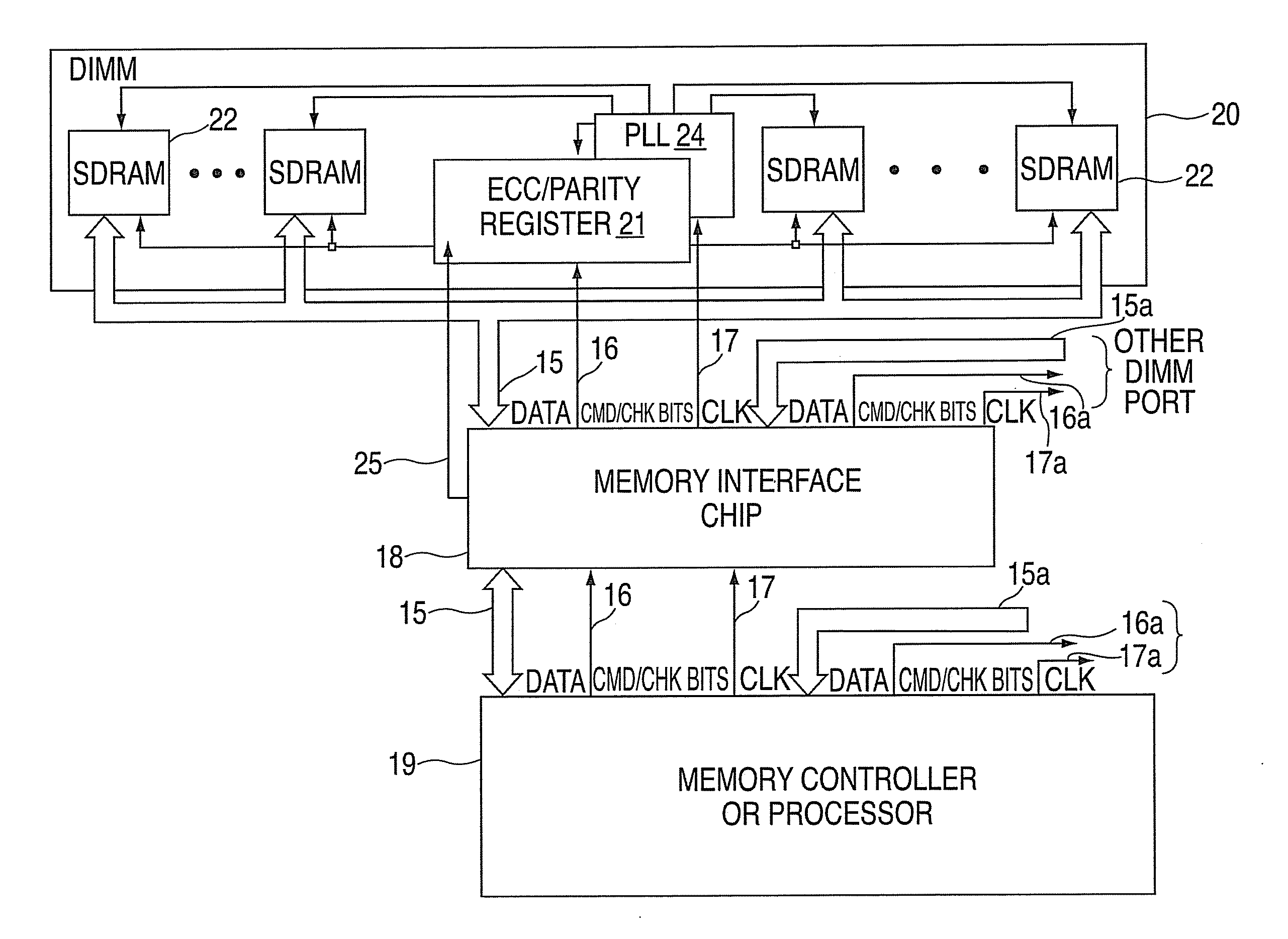
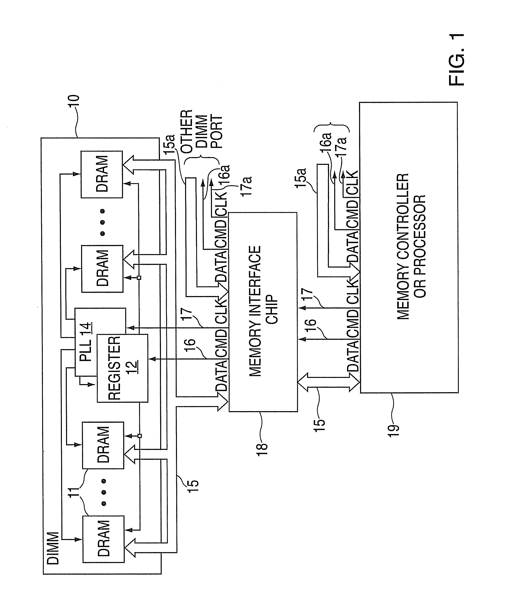
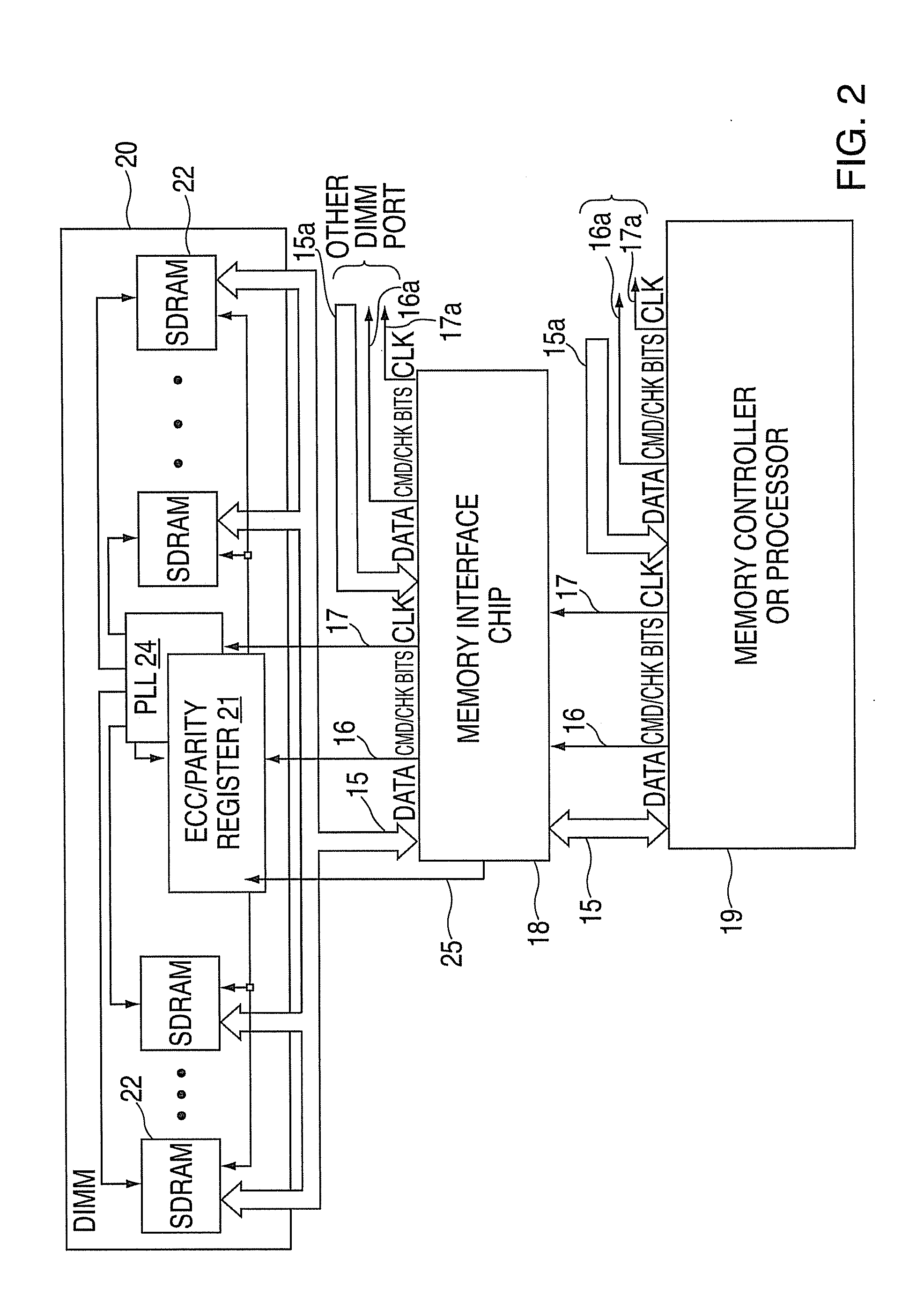
[0035]A full appreciation of the features and advantages of the present invention can best be gained by reference to the drawings and more particularly to the figures where: FIG. 1 is a block diagram of a typical server memory arrangement; FIG. 2 is a block diagram of the enhanced server memory arrangement of the present invention; FIGS. 3A and 3B are plan views respectively of the front and back of a 4 rank planar 276 contact dual inline memory module (DIMM) of the present invention; FIGS. 3C and 3D are plan views respectively of the front and back of a 4 rank four high stacked 276 contact DIMM of the present invention; FIGS. 4A and 4B are schematic views of the 4 rank-optimized buffer / register, parity and error correction circuits shown in FIGS. 3A and 3B (and FIGS. 3C and 3D); FIG. 5 is a block diagram of the single error correction / double error detection error correction code (SEC / DED ECC) circuit of FIG. 4B; FIG. 6 describes, in H—matrix, form the preferred ECC code selected fo...


PUM


Abstract

A high density high reliability memory module with power gating and a fault tolerant address and command bus. The memory module includes a rectangular printed circuit board having a first side and a second side, a length of between 149 and 153 millimeters and first and second ends having a width smaller than said length. The memory module also includes a first plurality of connector locations on the first side extending along a first edge of said board that extends the length of the board and a second plurality of connector locations on the second side extending on said first edge of said board. The memory module further includes a buffer device in communication with the circuit board for accessing up to four ranks of memory devices mounted on the first side and second side of the circuit board. In addition, a power savings means is included for causing all or a portion of the buffer device to be in an inactive mode in response to current activity at the memory module. The memory module also includes a locating key having its center positioned on said first edge and located between 82 mm and 86 mm from said first end of said card and located between 66 and 70 mm from said second end of said card.

Description

BACKGROUND OF THE INVENTION[0001]This invention relates generally to a high-density, high-reliability memory module with a fault tolerant address and command bus for use as a main memory that will achieve the degree of fault-tolerance and self-healing necessary for autonomic computing systems.[0002]Memory modules are well known to the prior art and have been and are presently being used in practical applications such as in computers and other equipment using solid state memories.[0003]Broadly speaking, currently available main memories offer bandwidths in the range of 1.6 to 2.6 GB / s, and although some memories provide for limited data path error correction most offer no means of any error correction targeting the interface between the memory controller and the memory subsystem. Furthermore, memory modules for server products and other higher-end computing systems usually include re-drive logic for address and command inputs, and clock re-synchronization and re-drive circuitry assoc...

Claims


Application Information

Patent Timeline
IPC IPC(8): H03M13/00
CPCH03M13/19G06F11/1044
Inventor HAZELZET, BRUCE G.
Owner IBM CORP
Why Eureka
Try Eureka