Low noise and high performance LSI device, layout and manufacturing method

a technology of low noise and high-performance, applied in the field of large-scale integration (lsi) semiconductor devices, can solve the problems of significant impact on power consumption and switching performance of the device, electrical noise, degrade the device performance, etc., and achieve the effect of reducing the effect of flicker noise on enhancing the performance of the devi

Active Publication Date: 2008-05-01
SAMSUNG ELECTRONICS CO LTD
View PDF13 Cites 17 Cited by
  • Summary
  • Abstract
  • Description
  • Claims
  • Application Information

AI Technical Summary

Benefits of technology

[0010] It is a feature of the invention to provide a semiconductor device such as an LSI device having mixed-signal applications, a layout of the semiconductor device and an approach to manufacturing the device, in which tensile and / or compressive stress are selectively applied to different portions of the device, i.e., analog and digital portions, to enhance performance of the device and simultaneously reduce the effects of flicker noise on the performance of the device.

Problems solved by technology

The carrier mobility in a MOS transistor has a significant impact on power consumption and switching performance of the device.
In addition to the improvement in carrier mobility, the introduction of mechanical stress into a MOS transistor has also been shown to degrade the performance of the device by introducing electrical noise, specifically, flicker noise.
Although the flicker noise is generated at relatively low frequencies, the noise may be very significant to some RF circuits since it is up-converted to the high frequency spectrum and degrades the coherency of oscillation.
That is, in both NMOS and PMOS devices, both tensile stress and compressive stress enhance performance of the devices but degrade the flicker noise characteristics of both devices.
Therefore, stress engineering is not always an acceptable means for improving overall circuit performance, when flicker noise characteristics are considered, such as, in particular, in analog applications, RF applications and mixed-signal applications, e.g., system LSI applications.

Method used


Image

  • Low noise and high performance LSI device, layout and manufacturing method
  • Low noise and high performance LSI device, layout and manufacturing method
  • Low noise and high performance LSI device, layout and manufacturing method

Examples


Embodiment Construction

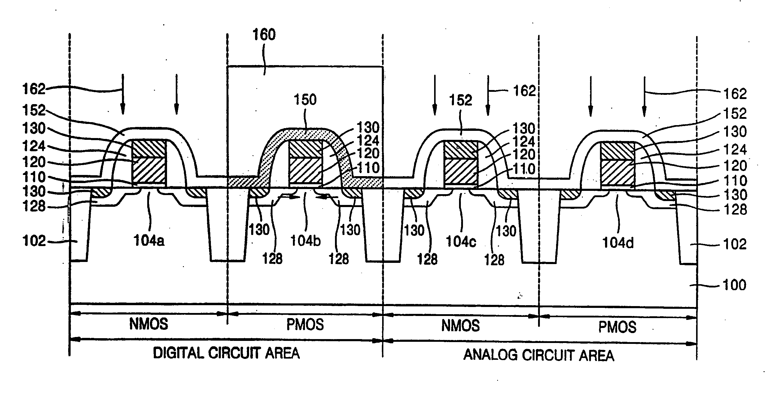
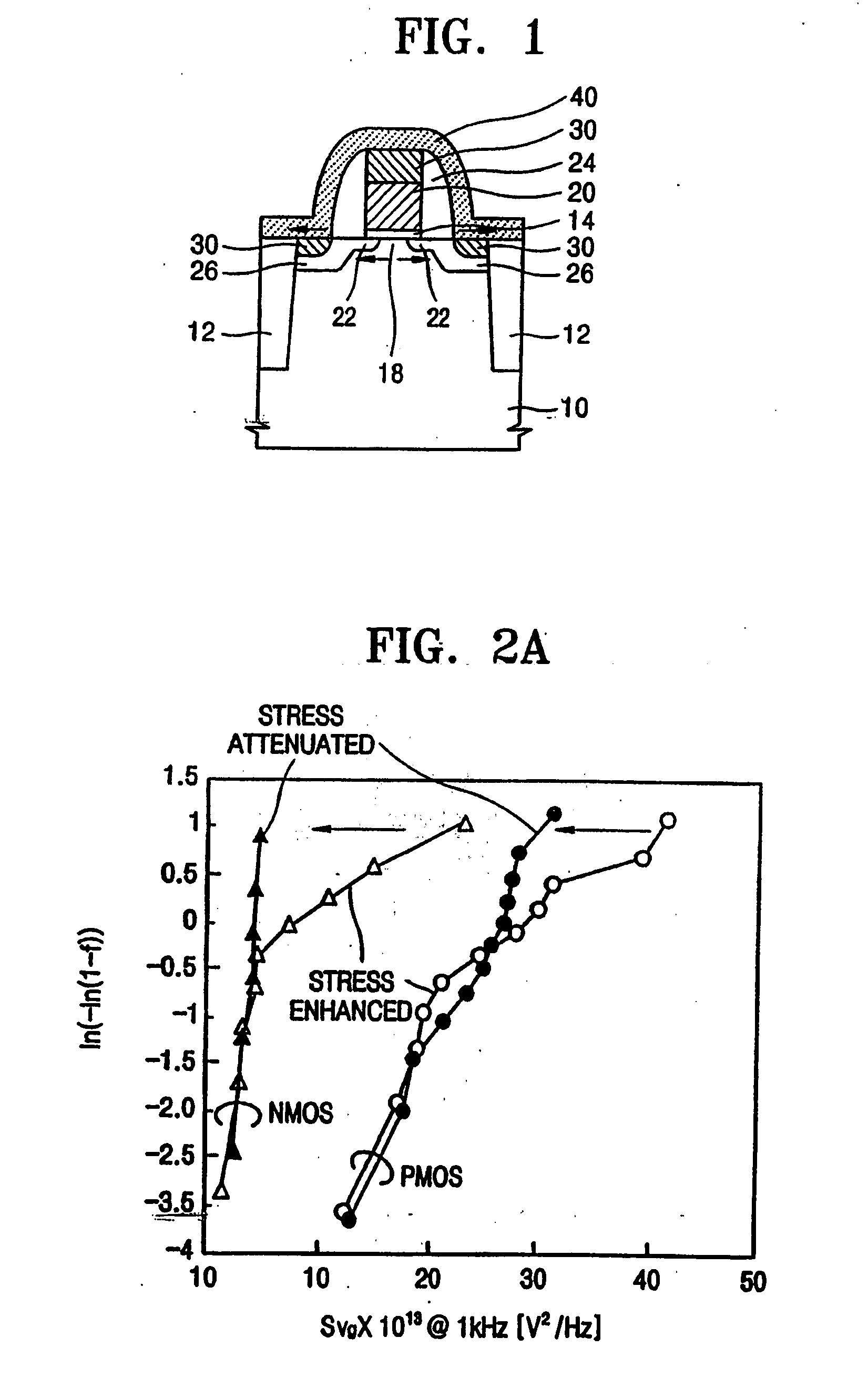
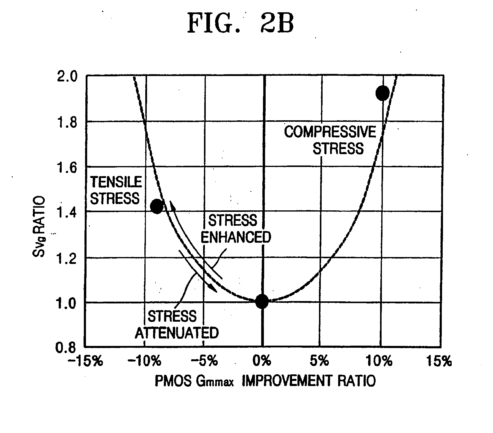
[0065] In accordance with the invention, a semiconductor device such as an LSI device having mixed-signal applications, i.e., analog and digital applications, a layout of the semiconductor device and an approach to manufacturing the device, in which tensile and / or compressive stress are selectively applied to different portions of the device, i.e., analog and digital portions, are provided to enhance performance of the device and simultaneously reduce the effects of flicker noise on the performance of the device.

[0066] In the following description, several embodiments of the invention are described. The various embodiments can be considered to belong to one of three categories of embodiments, the categories being defined by the general approach to selectively applying stress engineering to a device to enhance performance while limiting the effects of noise on the device. FIGS. 3 through 5 contain flow charts which illustrate the three categories, respectively, of the embodiments of...


PUM


Abstract

In semiconductor devices in which both NMOS devices and PMOS devices are used to perform in different modes such as analog and digital modes, stress engineering is selectively applied to particular devices depending on their required operational modes. That is, the appropriate mechanical stress, i.e., tensile or compressive, can be applied to and / or removed from devices, i.e., NMOS and / or PMOS devices, based not only on their conductivity type, i.e., n-type or p-type, but also on their intended operational application, for example, analog / digital, low-voltage / high-voltage, high-speed / low-speed, noise-sensitive / noise-insensitive, etc. The result is that performance of individual devices is optimized based on the mode in which they operate. For example, mechanical stress can be applied to devices that operate in high-speed digital settings, while devices that operate in analog or RF signal settings, in which electrical noise such as flicker noise that may be introduced by applied stress may degrade performance, have no stress applied.

Description

RELATED APPLICATION [0001] This application is a divisional of U.S. application Ser. No. 11 / 067,836, filed on Feb. 28, 2005, which relies for priority upon Korean Patent Application number 2004-0021569, filed in the Korean Intellectual Property Office on Mar. 30, 2004, the contents of which are incorporated herein in their entirety by reference.FIELD OF THE INVENTION [0002] The invention is directed to semiconductor devices and, more particularly, to Large Scale Integration (LSI) semiconductor devices, such as metal-oxide-silicon (MOS) transistors in which mechanical stress engineering is employed to improve device performance. BACKGROUND OF THE INVENTION [0003] The carrier mobility in a MOS transistor has a significant impact on power consumption and switching performance of the device. Improvement in carrier mobility allows faster switching speed and allows for operation at low voltages, resulting in reduced power consumption. [0004] Mechanical stress engineering has been employed...

Claims


Application Information

Patent Timeline
Patent Type & Authority Applications(United States)
IPC IPC(8): H01L27/092H01L21/336H01L21/82H01L21/8234H01L21/8238H01L21/8239H01L27/088H01L29/78
CPCH01L21/823412H01L21/823418H01L21/823807H01L21/823814H01L29/665H01L29/7845H01L29/7843H01L29/7848H01L27/1052H01L27/092H01L29/7833H10B99/00H01L27/0207H01L29/7842H01L27/0922H01L29/0649
Inventor MAEDA, SHIGENOBUYANG, JEONG HWAN
Owner SAMSUNG ELECTRONICS CO LTD
Why Eureka
Try Eureka