Semiconductor device and its manufacture method

a technology of semiconductors and manufacturing methods, applied in semiconductor devices, electrical devices, transistors, etc., can solve problems such as complex manufacturing processes, and achieve the effect of reducing the ion implantation conditions and simplifying the manufacturing process

Active Publication Date: 2008-05-01
FUJITSU SEMICON LTD
View PDF7 Cites 21 Cited by
  • Summary
  • Abstract
  • Description
  • Claims
  • Application Information

AI Technical Summary

Benefits of technology

[0024]The source/drain regions of one of NMOS and PMOS transistors are etched and dug and stress applying substance is buried, and epitaxial growth is performed for the other trans

Problems solved by technology

However, manufacture proc

Method used


Image

  • Semiconductor device and its manufacture method
  • Semiconductor device and its manufacture method
  • Semiconductor device and its manufacture method

Examples


Embodiment Construction

[0031]Embodiments of the present invention will now be described with reference to the accompanying drawings.

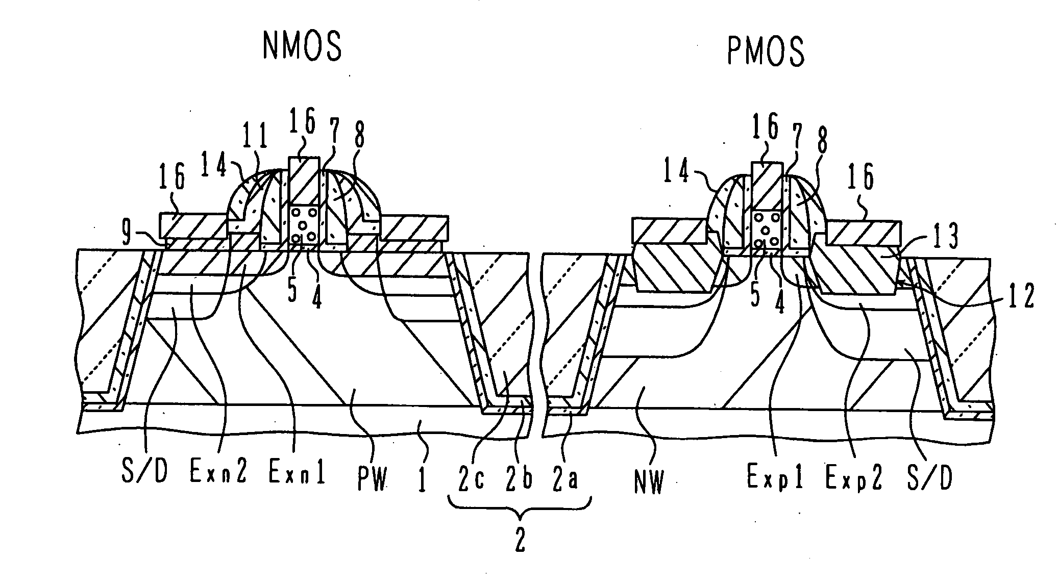
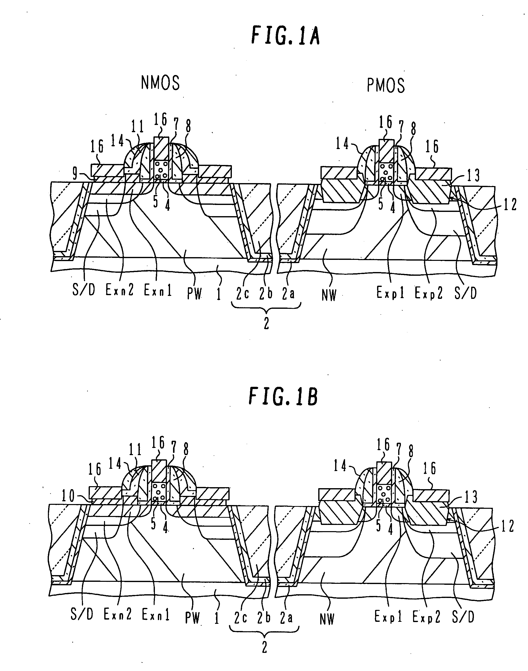
[0032]FIGS. 1A and 1B are cross sectional views schematically showing the structures of semiconductor devices according to the first and second embodiments.

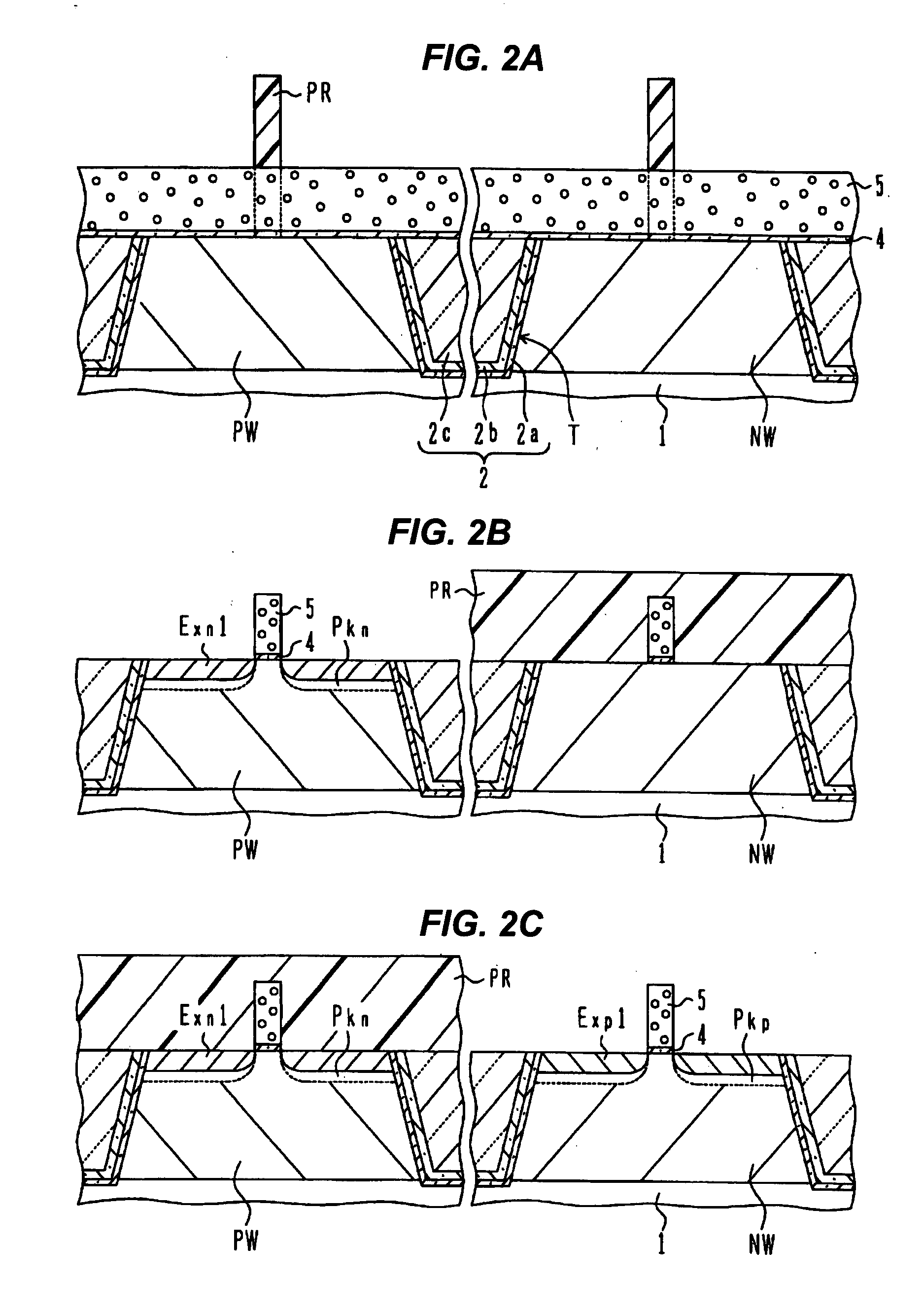
[0033]Referring to FIG. 1A, a p-type well PW and an n-type well NW are formed in the surface layer of a Si substrate 1 in active regions defined by an isolation region 2. For example, the isolation region 2 is formed by shallow trench isolation (STI) and made of a silicon oxide film liner 2a, a silicon nitride film liner 2b and a silicon oxide film 2c deposited by a high density plasma chemical vapor deposition (HDP-CVD) and made dense. An NMOS transistor is formed in the p-type well PW and a PMOS transistor is formed in the n-type well NW.

[0034]A gate electrode is formed traversing each of the active regions and made of a lamination of a gate insulating film 4, a polysilicon layer 5 and a silicide layer 16. First sidewall...


PUM


Abstract

A semiconductor device has a first MOS transistor formed on first active region of the first conductivity type, having first gate electrode structure, first source/drain regions, recesses formed in the first source/drain regions, and semiconductor buried regions buried and grown on the recesses for applying stress to the channel under the first gate electrode structure, and a second MOS transistor formed on second active region of the second conductivity type, having second gate electrode structure, second source/drain regions, and semiconductor epitaxial layers formed on the second source/drain regions without forming recesses and preferably applying stress to the channel under the second gate electrode structure. In a CMOS device, performance can be improved by utilizing stress and manufacture processes can be simplified.

Description

CROSS REFERENCE TO RELATED APPLICATION[0001]This application is based on and claims priority of Japanese Patent Application No. 2006-290773 filed on Oct. 26, 2006, the entire contents of which are incorporated herein by reference.BACKGROUND OF THE INVENTION[0002]A) Field of the Invention[0003]The present invention relates to a semiconductor device and its manufacture method, and more particularly to a semiconductor device having MOS transistors with stress applying mechanisms and its manufacture method. A field effect transistor having a gate electrode made of a lamination of a gate insulating film and a conductor film formed on a semiconductor active region is called a MOS transistor.[0004]B) Description of the Related Art[0005]Micro patterning has advanced in order to improve the integration density and operation speed of a silicon semiconductor integrated circuit. Micro patterning shortens the gate length of a MOS transistor. At a gate length of 65 nm or shorter, there is a limit...

Claims


Application Information

Patent Timeline
IPC IPC(8): H01L29/80H01L21/8238
CPCH01L21/823418H01L21/823807H01L21/823814H01L27/092H01L29/7848H01L29/6656H01L29/66636H01L29/7834H01L29/665
Inventor OHTA, HIROYUKI
Owner FUJITSU SEMICON LTD
Why Eureka
Try Eureka