Compound semiconductor substrate grown on metal layer, method for manufacturing the same, and compound semiconductor device using the same

a technology of compound semiconductor and metal layer, which is applied in the manufacture of semiconductor/solid-state devices, semiconductor devices, electrical devices, etc., can solve the problems of high-quality gan substrates that are difficult to manufacture, require much manufacturing cost and time, and require a large amount of process time, so as to improve light-emitting efficiency and reduce power consumption

Active Publication Date: 2008-05-08
LG SILTRON
View PDF13 Cites 21 Cited by
  • Summary
  • Abstract
  • Description
  • Claims
  • Application Information

AI Technical Summary

Benefits of technology

[0008] Therefore, the present invention is designed to solve the above-mentioned problems of the prior arts, and therefore it is an object of the present invention to provide a high quality and efficiency compound semiconductor substrate and a method for manufacturing the same simply and inexpensively.
[0014] As such, the manufacturing method of the present invention is performed by a simple and low price process without a delicate control.
[0017] Therefore, the compound semiconductor device of the present invention can use the metal layer both as a reflecting film and an electrode to achieve improvement of light emitting efficiency and reduction of power consumption.

Problems solved by technology

However, a high quality GaN substrate is very difficult to manufacture, and thus requires much manufacturing cost and time.
However, disadvantageously the ELO method goes through a complex process as mentioned above, requires much process time, and has problems in reproductibility and yield.
Meanwhile, it is also an important issue to achieve improvement of light emitting efficiency or reduction of power consumption of a light emitting device manufactured using the above-mentioned compound semiconductor.
That is, light generated from an active layer of a light emitting device is emitted toward a surface of the light emitting device and besides is emitted toward a substrate, so that the light is absorbed by the substrate, thereby reducing a light emitting efficiency.
However, this attempt has disadvantages of a complex process and much time required to make the patterned substrate.
However, essentially it is difficult to grow a GaN layer on a metal layer, and thus this U.S. patent uses such a costly process that defines a specific crystal face of an electrically insulating substrate having a single crystal structure as a surface to be layered, epitaxially grows a platinum layer on the specific face in the direction of a specific crystal orientation and epitaxially grows a GaN layer thereon.
As such, actually it requires a costly and complex process such as photolithography to manufacture a high quality compound semiconductor substrate with few crystal defects, and it requires a costly process to achieve improvement of light emitting efficiency and reduction of power consumption.
Further, in spite of high cost, problems of low reproductibility and yield are left unsettled.

Method used


Image

  • Compound semiconductor substrate grown on metal layer, method for manufacturing the same, and compound semiconductor device using the same
  • Compound semiconductor substrate grown on metal layer, method for manufacturing the same, and compound semiconductor device using the same
  • Compound semiconductor substrate grown on metal layer, method for manufacturing the same, and compound semiconductor device using the same

Examples


Embodiment Construction

[0019] Hereinafter, preferred embodiments of the present invention will be described in detail with reference to the accompanying drawings. Prior to the description, it should be understood that the terms used in the specification and the appended claims should not be construed as limited to general and dictionary meanings, but interpreted based on the meanings and concepts corresponding to technical aspects of the present invention on the basis of the principle that the inventor is allowed to define terms appropriately for the best explanation. In the case that the following description shows a layer exists on another layer, this may be interpreted that the layer may exist directly on another layer or a third layer may be interposed therebetween.

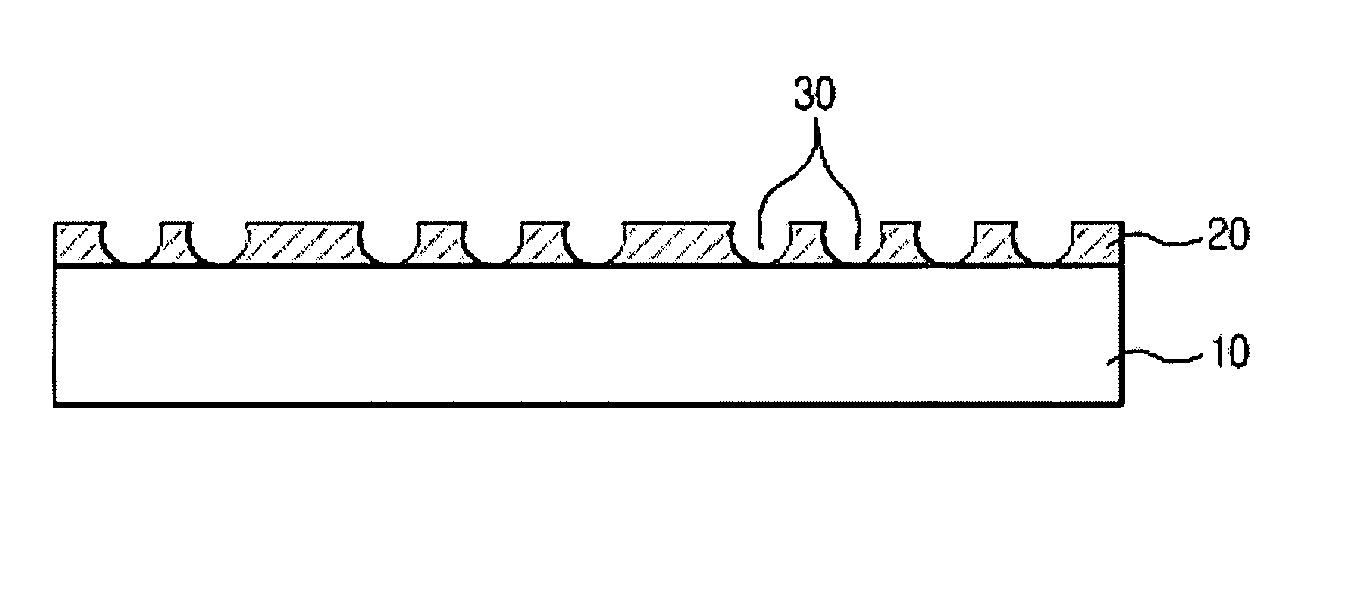
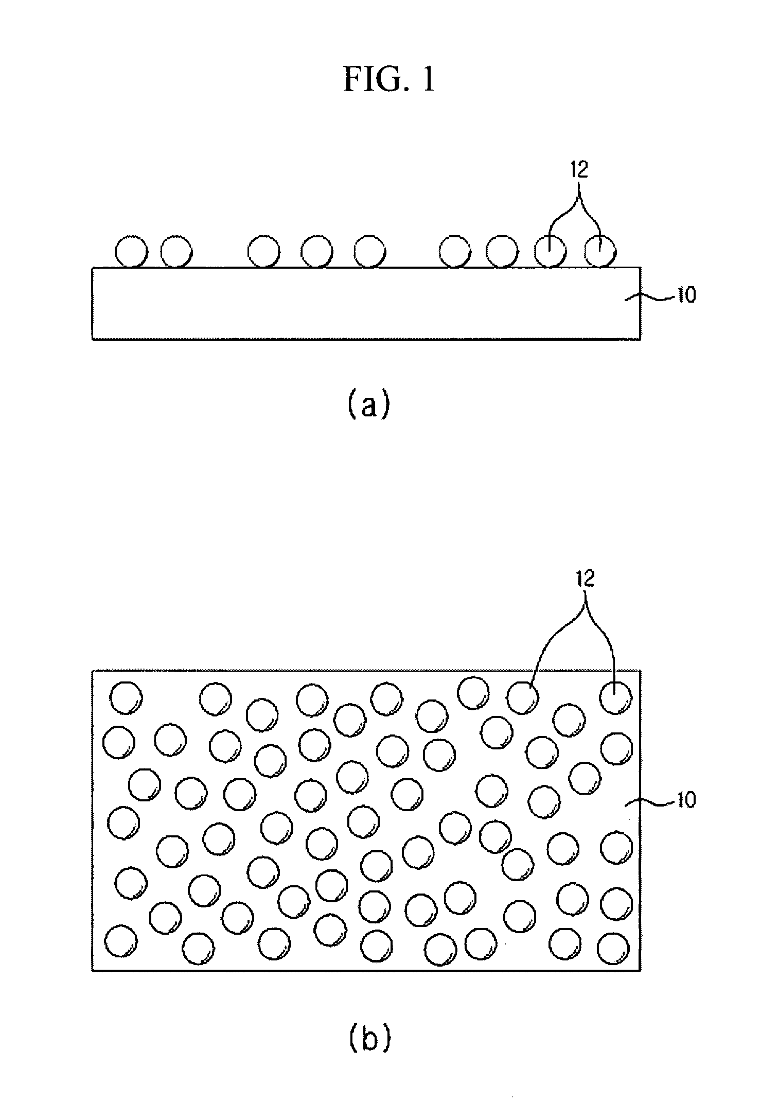
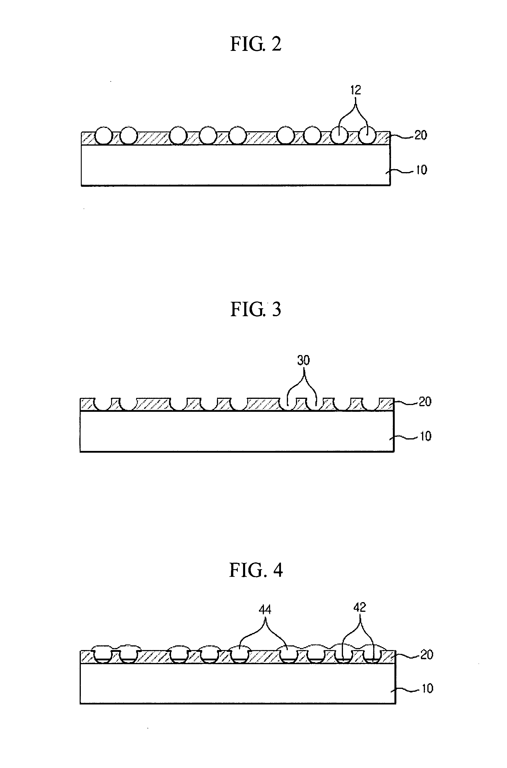
[0020] FIGS. 1 to 6 are schematic views illustrating a method for manufacturing a compound semiconductor substrate and a compound semiconductor device using the same according to a preferred embodiment of the present invention. FIG. 1 (a) ...


PUM

PropertyMeasurementUnit
diameteraaaaaaaaaa
thicknessaaaaaaaaaa
sizeaaaaaaaaaa

Abstract

The present invention relates to a compound semiconductor substrate and a method for manufacturing the same. The present invention provides the manufacturing method which coats spherical balls on a substrate, forms a metal layer between the spherical balls, removes the spherical balls to form openings, and grows a compound semiconductor layer from the openings. According to the present invention, the manufacturing method can be simplified and grow a high quality compound semiconductor layer rapidly, simply and inexpensively, as compared with a conventional ELO (Epitaxial Lateral Overgrowth) method or a method for forming a compound semiconductor layer on a metal layer. And, the metal layer serves as one electrode of a light emitting device and a light reflecting film to provide a light emitting device having reduced power consumption and high light emitting efficiency.

Description

BACKGROUND OF THE INVENTION [0001] 1. Field of the Invention [0002] The present invention relates to a compound semiconductor substrate used in manufacturing a light emitting device and a method for manufacturing the same, and in particular, to a method for manufacturing a compound semiconductor substrate, which is capable of manufacturing a semiconductor substrate having a compound semiconductor layer grown on a metal layer easily and inexpensively, and to a compound semiconductor substrate and a compound semiconductor device manufactured thereby. [0003] 2. Description of the Related Art [0004] Gallium nitride (GaN) as a typical compound semiconductor is known as a material suitable for application to a blue light emitting device or a high temperature electronic device. Recently, as the blue light emitting device is a sharp rise in demand, a demand for a GaN substrate is increasing. However, a high quality GaN substrate is very difficult to manufacture, and thus requires much manuf...

Claims


Application Information

Patent Timeline
Patent Type & Authority Applications(United States)
IPC IPC(8): H01L33/00H01L29/06H01L21/205H01L33/12H01L33/32H01L33/44
CPCH01L21/0237H01L21/02458H01L21/0254H01L21/02573H01L33/38H01L21/02642H01L21/02647H01L33/20H01L21/02639
Inventor KIM, YONG-JINKIM, DOO-SOOLEE, HO-JUNLEE, DONG-KUN
Owner LG SILTRON
Why Eureka
Try Eureka