Manufacturing Method of Semiconductor Device

a manufacturing method and semiconductor technology, applied in the field of manufacturing methods of semiconductor devices, can solve the problems of increased cost and decreased throughput, and achieve the effects of improving throughput, reducing manufacturing costs, and simplifying the process of forming an opening

Inactive Publication Date: 2008-05-08
SEMICON ENERGY LAB CO LTD
View PDF19 Cites 52 Cited by
  • Summary
  • Abstract
  • Description
  • Claims
  • Application Information

AI Technical Summary

Benefits of technology

[0029] By using the present invention, an opening can be formed in a thin film such as an insulating layer without using a photoresist. Therefore, a process of forming an opening can be simplified in a manufacturing process of a semiconductor device, which enables reduction in manufacturing cost and improvement in throughput.

Problems solved by technology

Therefore, the cost is increased and the throughput is decreased as the number of lithography steps is increased.

Method used


Image

  • Manufacturing Method of Semiconductor Device
  • Manufacturing Method of Semiconductor Device
  • Manufacturing Method of Semiconductor Device

Examples


embodiment mode 1

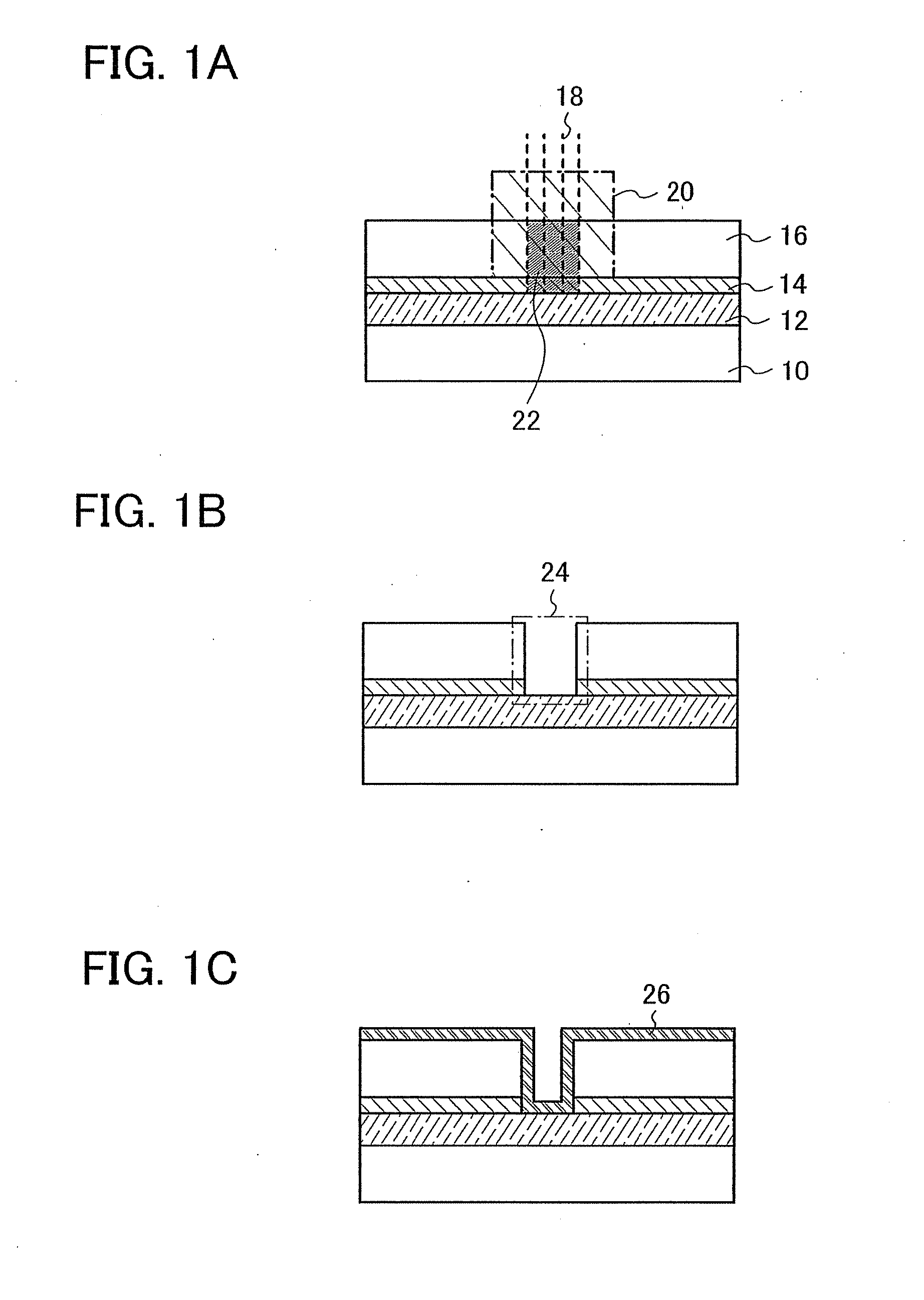
[0065] One feature of the present invention is to form an opening in a desired region without using a lithography technique that uses a photoresist. In Embodiment Mode 1, an opening for electrically connecting conductive layers to each other is formed in an irradiation object. Hereinafter, one mode of a method for forming an opening in an irradiation object by application of the present invention will be described with reference to FIGS. 1A to 3C.

[0066]FIG. 1A shows an example of a structure of an irradiation object in which an opening is formed using the present invention. The irradiation object has a structure where a conductive layer 12, a first material layer 14, and a second material layer 16 are sequentially stacked over a substrate 10. The irradiation object is irradiated with a first laser beam 18 and a second laser beam 20 from the second material layer 16 side so that the first laser beam 18 and the second laser beam 20 overlap. In the irradiation object, a region irradia...

embodiment mode 2

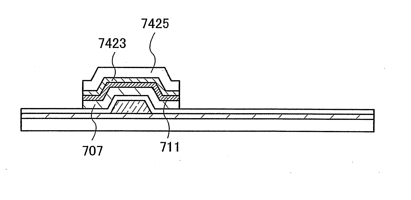
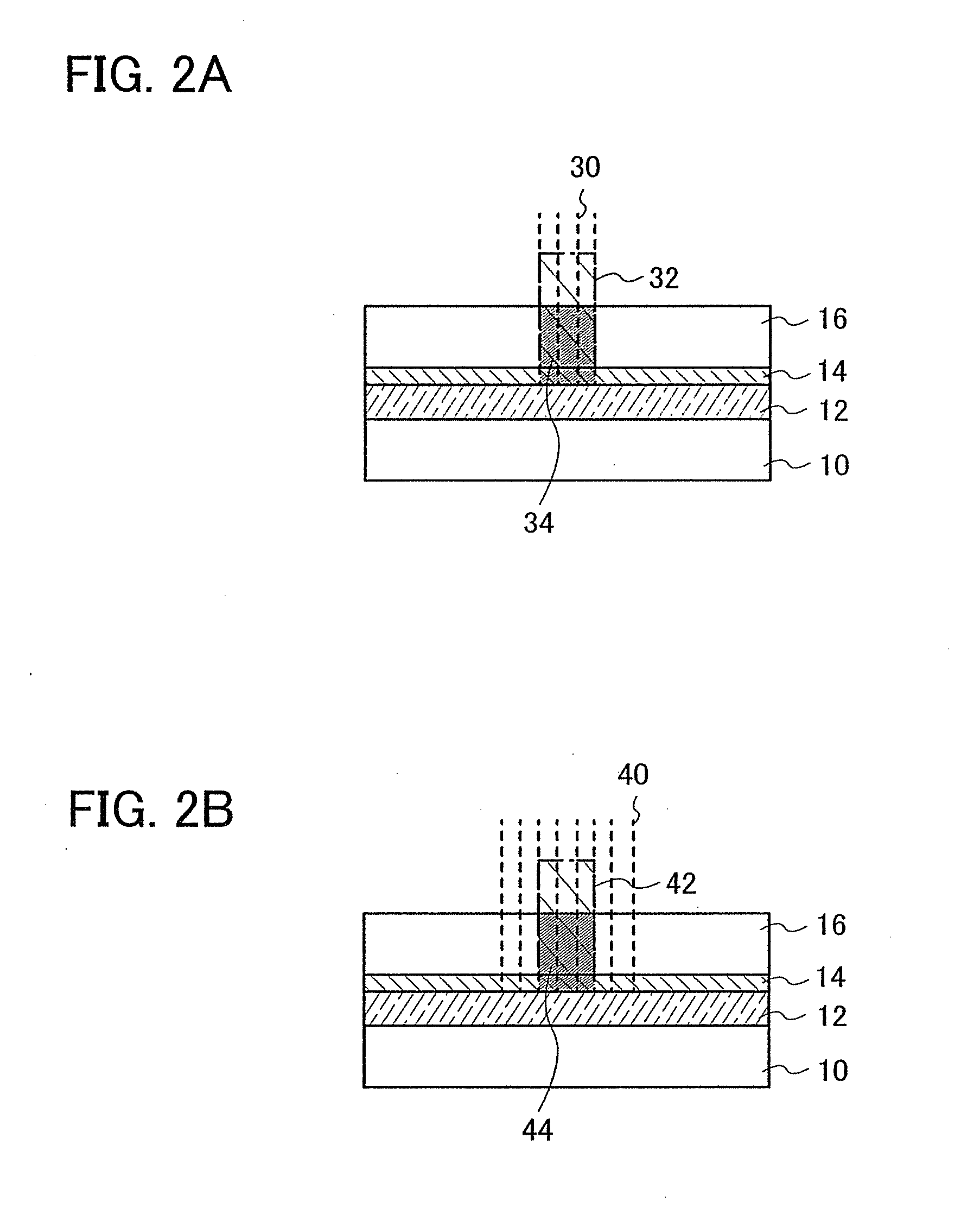
[0091] Embodiment Mode 2 will describe a method of forming an opening which electrically connects conductive layers to each other or connects a conductive layer to a semiconductor layer in an irradiation object. Embodiment Mode 1 shows an example where an opening is formed to penetrate the first material layer and the second material layer stacked over the conductive layer and the conductive layer is exposed at the bottom of the opening. In this embodiment mode, another example of forming an opening which reaches a conductive layer is shown. In addition, an example of forming an opening which reaches a semiconductor layer is also shown.

[0092]FIGS. 7A to 7C show structures, in each of which an opening reaching a conductive layer or a first material layer is formed in an irradiation object which is formed by sequentially stacking the conductive layer, the first material layer, and a second material layer over a substrate. In addition, a conductive layer is formed in the opening, and ...

embodiment mode 3

[0113] Embodiment Mode 3 will describe a structural example of a laser processing apparatus of the present invention.

[0114]FIG. 11 is a pattern diagram showing a structure of a laser processing apparatus according to the present invention. The laser processing apparatus according to the present invention includes a first laser 3120 and a second laser 3130. A first laser beam 3122 is emitted from the first laser 3120. A second laser beam 3132 is emitted from the second laser 3130. The traveling direction, the polarization direction, and the like of the laser beams (first laser beam 3122 and second laser beam 3132) emitted from the lasers (first laser 3120 and second laser 3130) are controlled by an optical system which is a combination of mirrors and a condenser lens, so that an irradiation object is irradiated with the overlapping laser beams. Specifically, the traveling direction, polarization direction, and the like of the first laser beam 3122 emitted from the first laser 3120 a...


PUM

PropertyMeasurementUnit
oscillation wavelengthaaaaaaaaaa
wavelengthaaaaaaaaaa
thicknessaaaaaaaaaa

Abstract

In a manufacturing process of a semiconductor device, a manufacturing technique of a semiconductor device by which a lithography step that uses a photoresist is simplified is provided. A manufacturing cost is reduced and throughput is improved. An irradiation object is formed over a substrate by sequentially stacking a first material layer and a second material layer. The irradiation object is irradiated with a first laser beam that is absorbed by the first material layer and a second laser beam that is absorbed by the second material layer so that the laser beams overlap. A part or all of the region irradiated with an overlap part of the laser beams is ablated to form an opening.

Description

BACKGROUND OF THE INVENTION [0001] 1. Field of the Invention [0002] The present invention relates to a manufacturing method of a semiconductor device. In particular, the present invention relates to a method of forming an opening in a thin film such as a conductive layer or an insulating layer. [0003] 2. Description of the Related Art [0004] In a conventional technique, thin films such as an insulating layer and a conductive layer are formed over a substrate and a desired pattern is formed by a lithography technique, as appropriate, so as to manufacture a MOS transistor, a thin film transistor (hereinafter also referred to as a TFT), and a semiconductor device including such a transistor. A lithography technique is a technique in which a pattern of a circuit or the like called a photomask, which is formed with a light-blocking material over a transparent flat plate, is transferred to an aimed object by utilizing light. The lithography technique has been widely used in a process of m...

Claims


Application Information

Patent Timeline
Patent Type & Authority Applications(United States)
IPC IPC(8): H01L21/02
CPCB23K26/0613B23K26/409H01L27/1288H01L27/124H01L21/76802B23K26/40B23K2103/172G03F7/2053H01L21/0274H01L27/1214
Inventor TANAKA, KOICHIROYAMAZAKI, SHUNPEI
Owner SEMICON ENERGY LAB CO LTD
Why Eureka
Try Eureka