Stencil design and method for cell projection particle beam lithography

a particle beam lithography and stencil technology, applied in the field of particle beam lithography, can solve the problems of low manufacturing yield, difficult accurate transcription, and significant optical proximity effect, and achieve the effect of reducing the eb writing tim

a particle beam lithography and stencil technology, applied in the field of particle beam lithography, can solve the problems of low manufacturing yield, difficult accurate transcription, and significant optical proximity effect, and achieve the effect of reducing the eb writing tim

US20080116397A1Active Publication Date: 2008-05-22ADVANTEST CORP

Image

  • Stencil design and method for cell projection particle beam lithography
  • Stencil design and method for cell projection particle beam lithography
  • Stencil design and method for cell projection particle beam lithography

Examples


Embodiment Construction

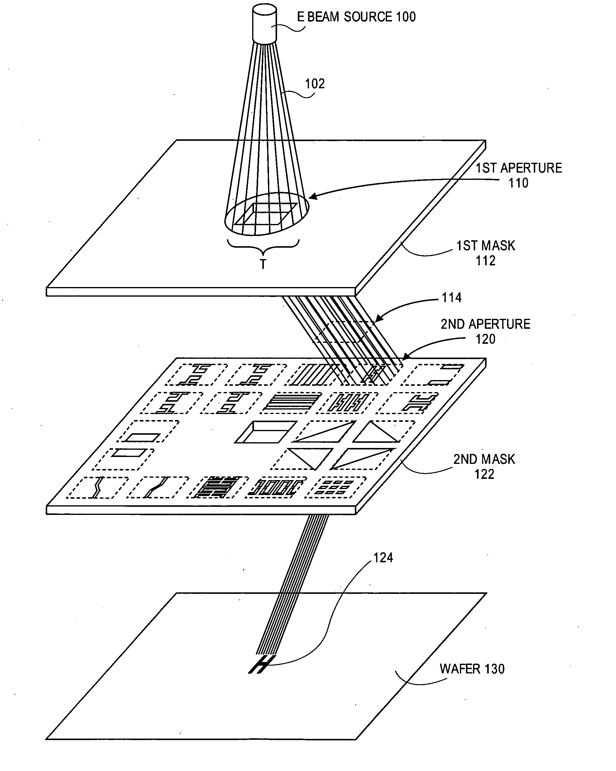
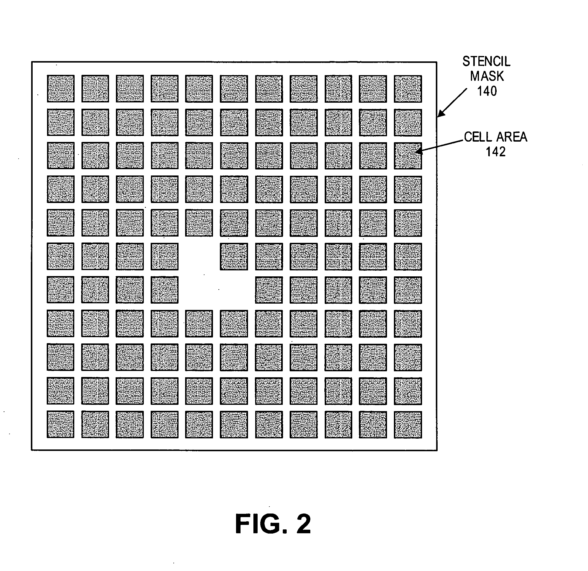
[0036]Various embodiments of the invention are described herein with reference to the drawings. It should be noted that the drawings are not drawn to scale and that elements of similar structures or functions are represented by like reference numerals throughout the drawings.

[0037]The following discussion describes EB direct writing (EBDW) as an application of particle beam lithography and should not be limited to only EB direct writing (EBDW), but the this invention can be applied to mask writing using an electron beam (EB) writer with cell projection (CP) capability, in a similar manner, resulting in an improved throughput.

[0038]Accordingly, it should be appreciated that this invention may also be applied to other drawing technologies with transcribed patterns using at least two apertures (stencil masks) and using other types of particle beams other than an electron beam (EB), such as an optical (light) laser beam, an X-ray beam or any other particle beams that run straight and st...


PUM

PropertyMeasurementUnit
areaaaaaaaaaaa
areaaaaaaaaaaa
shapeaaaaaaaaaa

Abstract

A method and system for particle beam lithography, such as electron beam (EB) lithography, is disclosed. The method and system include selecting one of a plurality of cell patterns from a stencil mask and partially exposing the cell pattern to a particle beam, such as an electron beam, so as to selectively project a portion of the cell pattern on a substrate.

Description

RELATED APPLICATIONS[0001]This application is related to co-pending U.S. Patent Application entitled, “Method and System for Improving Particle Beam Lithography”, Attorney Docket No. CA7050002001, filed concurrently herewith, the entire disclosure of which is expressly incorporated by reference herein.BACKGROUND[0002]1. Field[0003]The field of the present invention relates to particle beam lithography, and in particular to stencil design and a method for cell projection particle beam lithography.[0004]2. Description of Related Art[0005]In current semiconductor manufacturing processes, optical lithography with photomasks is commonly used. Photomasks consist of a glass substrate and mask patterns drawn on it and are commonly used to form device patterns on a silicon wafer. However, as the feature size becomes smaller than the wavelength of the ultraviolet light, which is used to optically transcribe mask patterns onto a silicon wafer, optical proximity effect becomes significant and a...

Claims


Application Information

Patent Timeline
22 May 2008
Publication
US20080116397A1
IPC
H01J37/30; G03B27/58; G21K5/04; G21K1/02; G03F1/16
CPC
B82Y10/00; H01J37/3174; G03F1/20; B82Y40/00
Inventors
YOSHIDA, KENJI; MITSUHASHI, TAKASHI