Method and system for proximity effect and dose correction for a particle beam writing device

a particle beam and proximity effect technology, applied in the field of particle beam writing and lithograph technologies, can solve the problems of image quality degradation and resolution limits, degradation or difference between obtained image and intended pattern, and limited size of cp cells on stencil plates,

Inactive Publication Date: 2008-05-22
CADENCE DESIGN SYST INC
View PDF17 Cites 100 Cited by
  • Summary
  • Abstract
  • Description
  • Claims
  • Application Information

AI Technical Summary

Benefits of technology

[0020]The invention presented herein relates to particle beam writing, lithograph technologies for fine image fabrication, and proximity effect correction. Examples of lithography technology by a particle beam writer include, but are not limited to, an electron beam (EB) writing device, an X-ray writing device and an optical (light) laser beam writing device. One fundamental problem with conventional photolithography technology is the image quality degradation from the intended patterns that is caused by proximity effects. This problem can be solved by a technology referred to as proximity effect correction.

Problems solved by technology

A fundamental problem with conventional lithograph technologies is image quality degradation and resolution limits caused by chemical and physical effects in the process of the technologies.
The degradation or difference between obtained image and intended pattern becomes serious with fine images.
Proximity effect is one of the most dominant issues among these effects.
However, the size of CP cells on the stencil plate has limitations.
PEC by a pattern method is not suitable for VSB type EB writers because pattern modification or auxiliary patterns increase the number of shots required, and as a result, writing time becomes longer.
On the other hand, by using CP cell type writer, plural patterns are written by one CP shot and dose correction among patterns in the CP cell or to use different dose for writing patterns in the CP cell is generally difficult to achieve.
As a result of the above mentioned discussion, a problem occurs in which the width of the obtained images vary depending on the position in the CP cell 400, although target width is identical among those patterns.
Computing time is another issue for PEC.
However, the area density (AD) method is not an accurate approximation.
Another issue is that the division of a chip by the grid does not fit to the idea of writing by CP cell.
Conventionally, the scattering effect caused by reflection or collision of particles or electrons with wiring or via / contact material is not considered enough.
However, the conventional solutions are not practical because procedures for taking underlay structure effect into account are tedious and time consuming.
Other aspects of this issue is that combination of vias and wires is diverse in structure and difficult to handle by a computer.
The reason for this weakness is that size and position of exposed regions by CP and VSB writing is not aligned with the model for scattering so that the scattering model is not directly usable for the writing.
However, it is not suitable to use layout patterns itself for generating the model because the patterns have diverse configurations.
One fundamental problem with conventional photolithography technology is the image quality degradation from the intended patterns that is caused by proximity effects.

Method used


Image

  • Method and system for proximity effect and dose correction for a particle beam writing device
  • Method and system for proximity effect and dose correction for a particle beam writing device
  • Method and system for proximity effect and dose correction for a particle beam writing device

Examples


Embodiment Construction

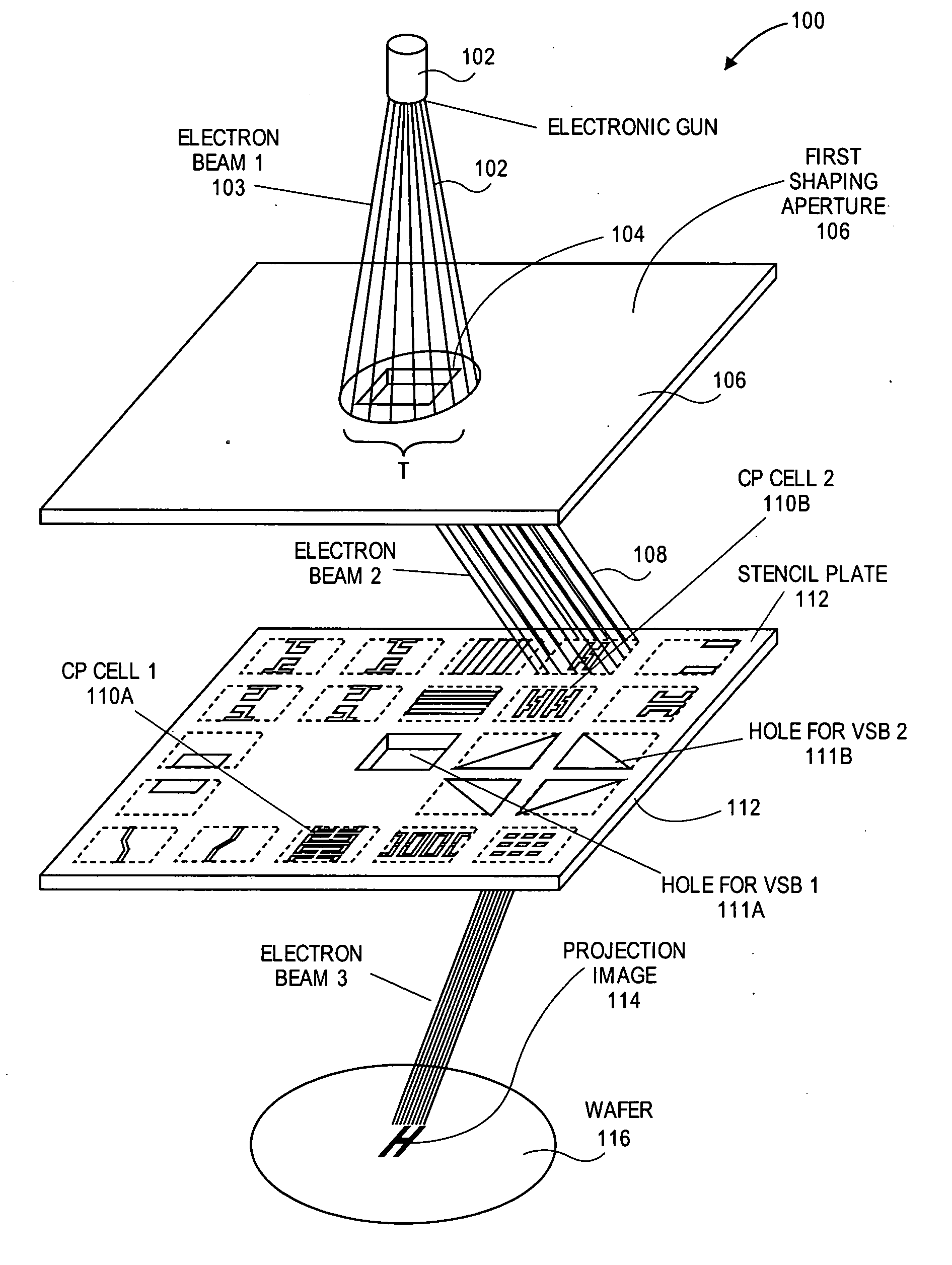
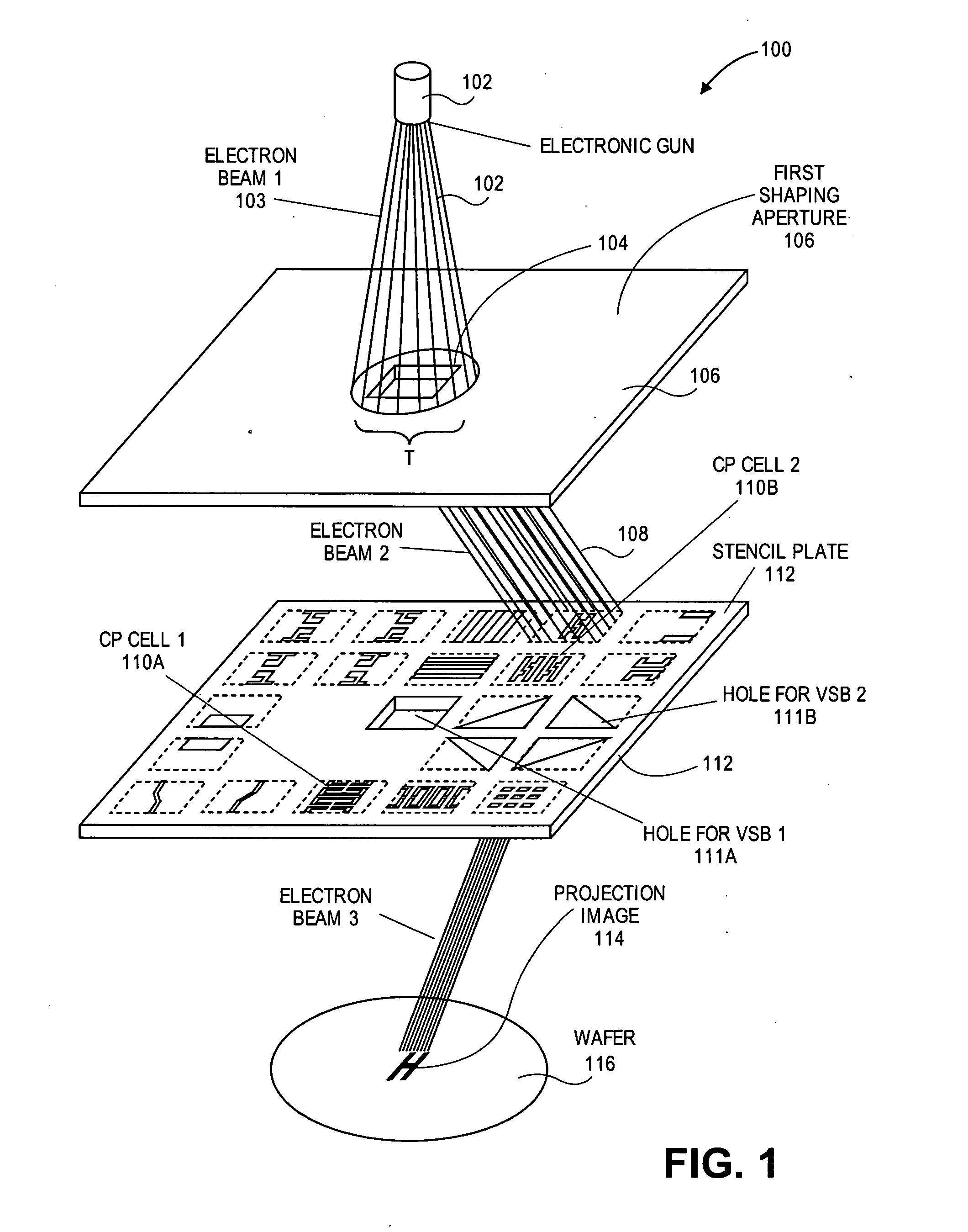
[0070]Various embodiments of the invention are described herein with reference to the drawings. It should be noted that the drawings are not drawn to scale and that elements of similar structures or functions are represented by like reference numerals throughout the drawings.

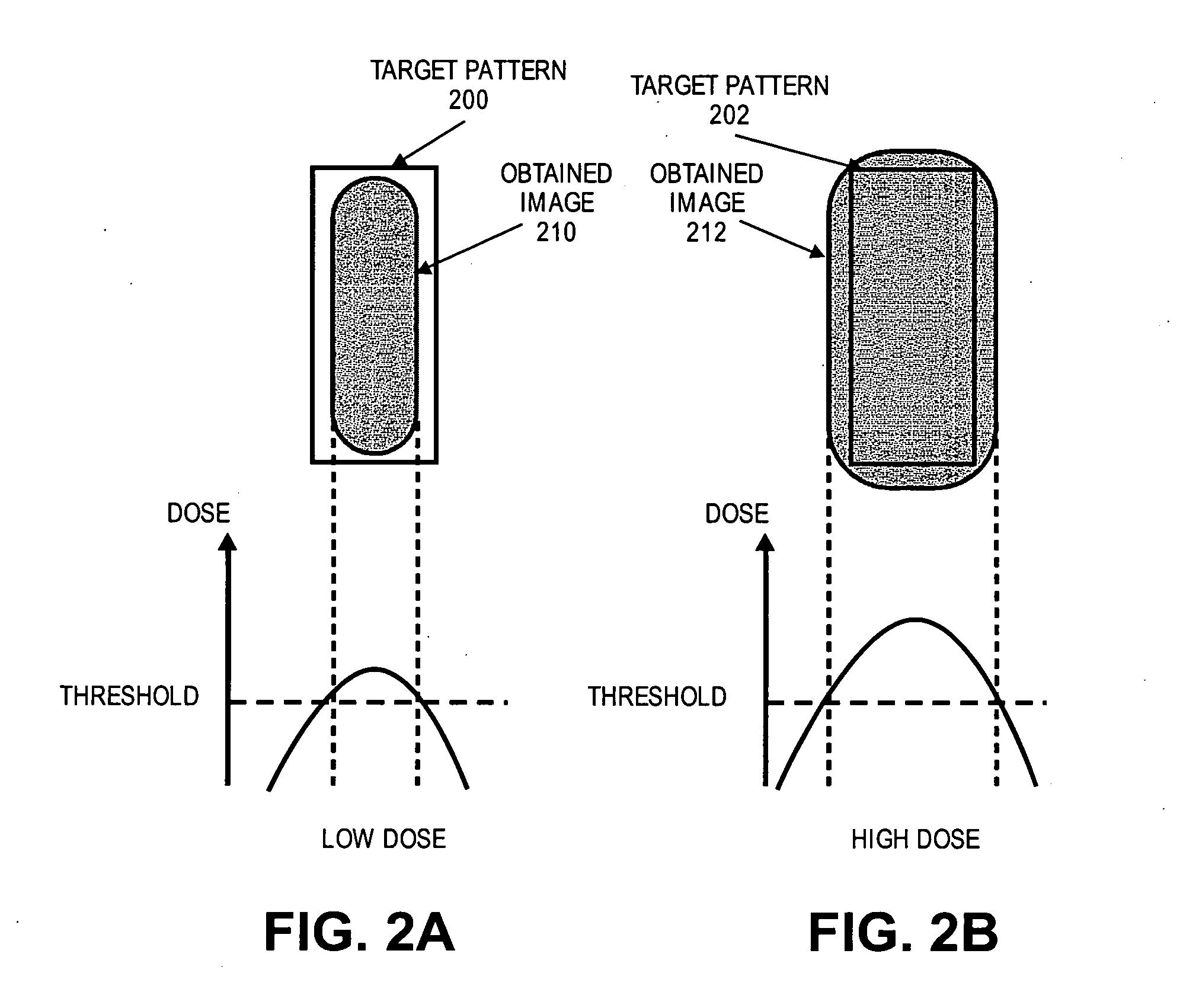
[0071]In one embodiment, the invention uses both proximity effect correction by pattern modification and proximity effect correction by dose. A first step of this procedure matches an assumed dose quantity for PEC by pattern modification to the threshold of deposit energy that determines appearance of lithography pattern. In a next step, PEC by pattern modification is applied to CP cells. The following steps will be done for all polygons in a CP cell of interest.

[0072](1) A polygon is broken into a set of line segments that are boundaries of the polygon.

[0073](2) Evaluation points are set on the segments so that differences between target and obtained value of deposit energy at the evaluation points can be calcu...


PUM


Abstract

A method of particle beam lithography includes selecting at least two cell patterns from a stencil, correcting proximity effect by dose control and by pattern modification for the at least two cell patterns, and writing the at least cell two patterns by one shot of the particle beam after proximity effect correction (PEC).

Description

BACKGROUND[0001]1. Field[0002]The field of the present invention relates to particle beam writing and lithograph technologies for fine image fabrication and, in particular, to a method and system for proximity effect and dose correction for a particle beam writing device.[0003]2. Description of Related Art[0004]In conventional semiconductor manufacturing processes for generating fine images on a plate by lithography, technologies like particle beam writers and an optical projection lithography method that uses a mask consisting of transparent and opaque parts have been used. The plate is coated by a particle beam sensitive resist. An example of a particle beam writer is an electron beam (EB) writer, which is used for writing fine images on both silicon wafers and glass masks for optical projection lithography. A technology that uses electron beam (EB) writers for making fine images for semiconductor integrated circuits directly on the semiconductor wafer is electron beam direct writ...

Claims


Application Information

Patent Timeline
Patent Type & Authority Applications(United States)
IPC IPC(8): G06F17/50H01J37/30G21K5/04
CPCB82Y10/00B82Y40/00H01L21/0278H01L21/0275H01L21/0277H01J37/3174Y10S430/143
Inventor HARA, DAISUKEKOMURO, KATSUOMITSUHASHI, TAKASHI
Owner CADENCE DESIGN SYST INC
Why Eureka
Try Eureka