Source-coupled differential low-swing driver circuits

Inactive Publication Date: 2008-05-22
NAIR RAJENDRAN
View PDF7 Cites 4 Cited by
  • Summary
  • Abstract
  • Description
  • Claims
  • Application Information

AI Technical Summary

Benefits of technology

[0006]The invention improves upon prior art substantially through a novel source-coupled differential low-swing (SCDL) driver circuit. Output signals are connected to the source terminals of driving switches in the invention circuit, minimizing the detrimental impact of miller coupling capacitance between gate nodes and driven output nodes upon output slew-rate, enabling higher frequencies of operation. Output signal

Problems solved by technology

These are undesirable characteristics of DVI electrical and physical layers and TMDS that necessitate high quality and associated cost in video cable construction in order to maintain acceptable bit error rates.
Prior art TMDS CMOS drivers as illustrated in FIG. 1 have significant functional disadvantages that impact output signal integrity.
This leads to a slower overall ‘slew-rate’ or rate of change of the output, limiting high-spee

Method used


Image

  • Source-coupled differential low-swing driver circuits
  • Source-coupled differential low-swing driver circuits
  • Source-coupled differential low-swing driver circuits

Examples


Example

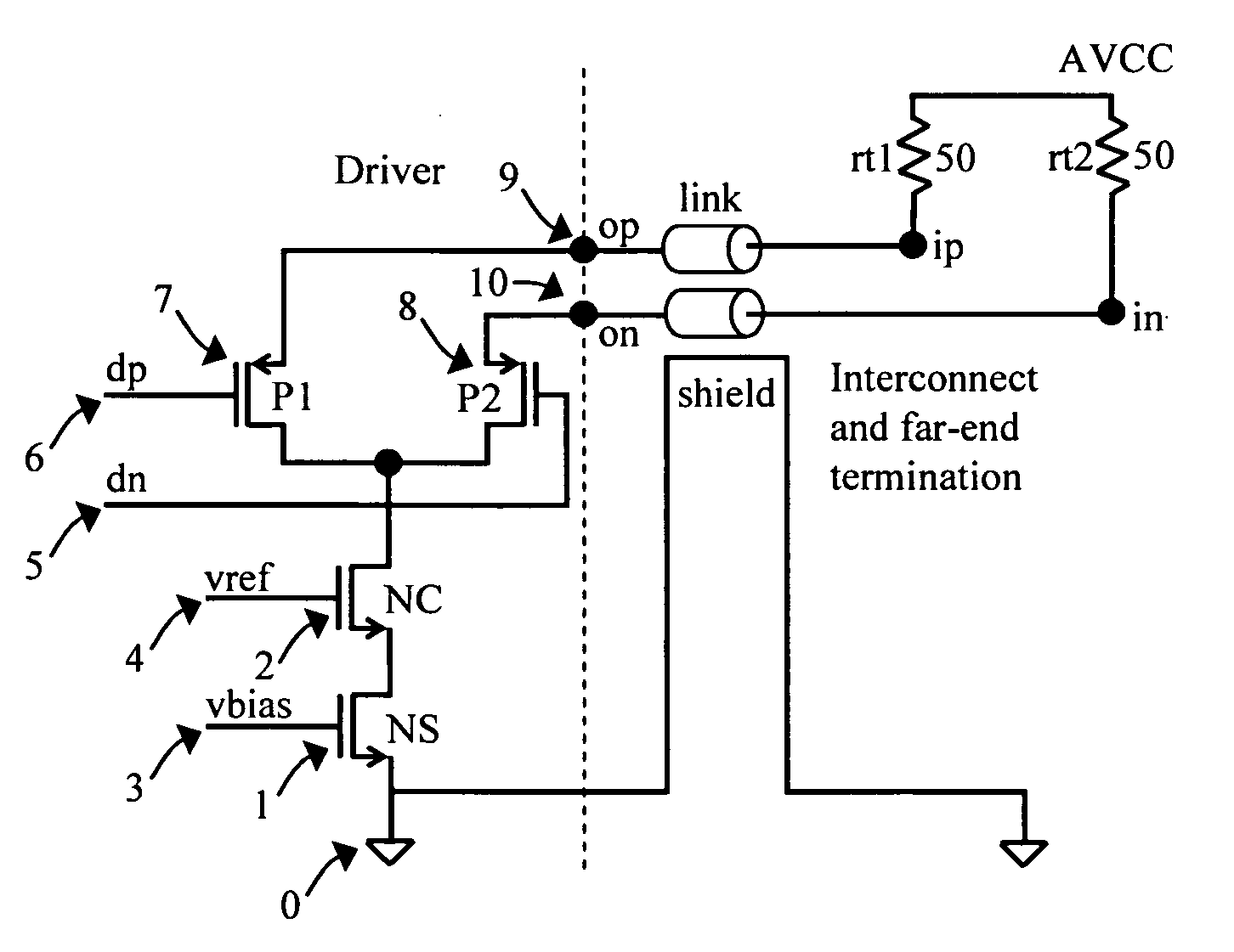
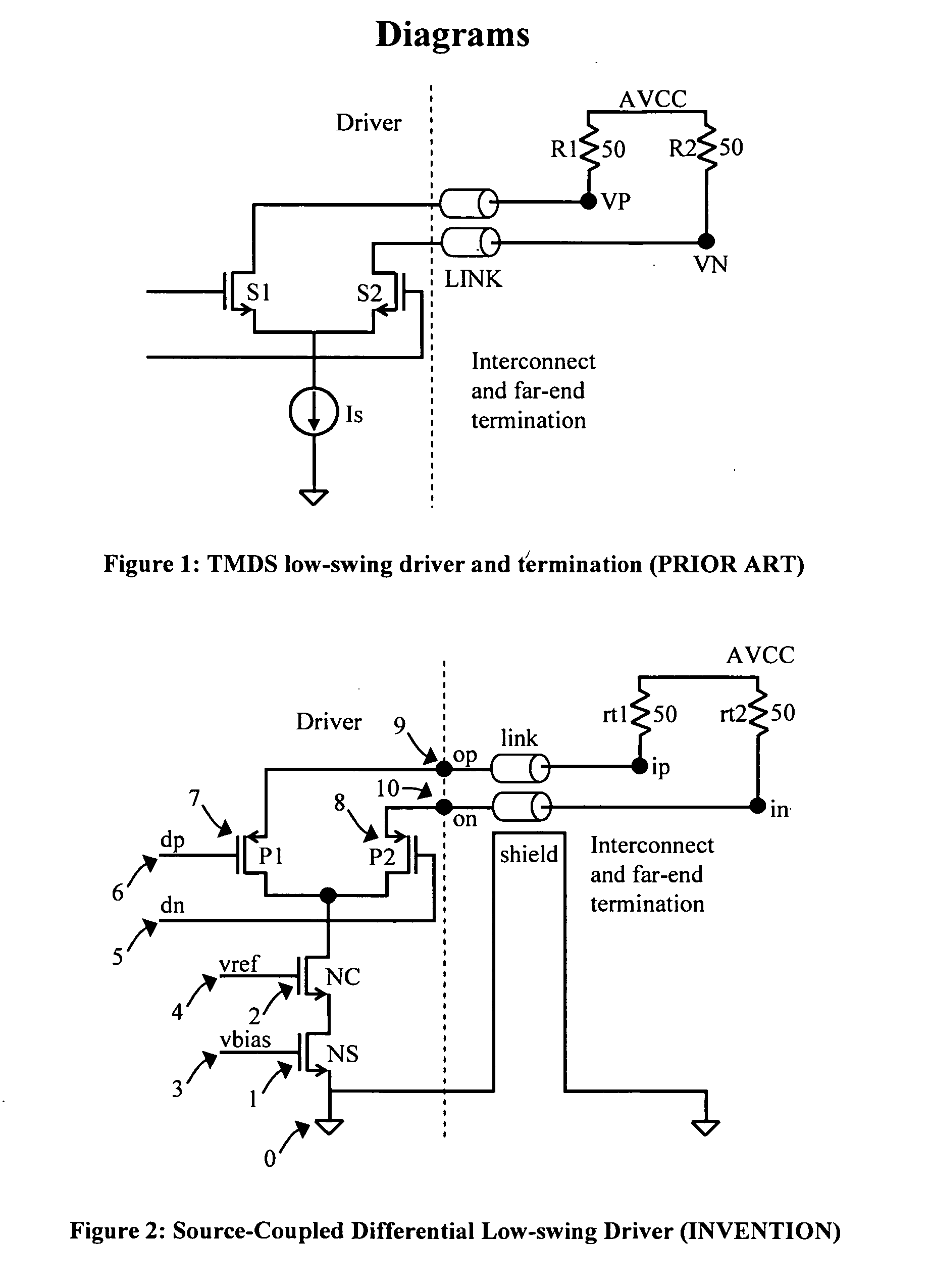
[0011]A prior art embodiment of a TMDS differential signaling output driver and termination architecture is illustrated in FIG. 1. In this driver implemented in CMOS technology, a tail current source connects through two NFET switch devices to output signal wires which are terminated at the far-end of the cable in a single-ended manner to a common reference power supply AVCC. When switch S1 turns ‘off’ and S2 turns ‘on’ driven by input signals to the gates of these devices, the current source current Is is diverted to flow through the output signal wire connecting to far-end node VN and through terminating resistance R2, thereby pulling node VN lower by a voltage value corresponding to the product of the current and the terminating resistance. In typical embodiments of the prior art, the terminating resistors are 50 Ohms in value and the current source is 10 mA, resulting in a 500 mV drop in voltage. Simultaneously, since switch S1 turns ‘off’, no current flows through the output si...


PUM


Abstract

A novel source-coupled differential driver circuit fully compatible with digital visual interface TMDS signaling specification is disclosed. Driven output signals are connected to the source terminals of driving switches in the invention circuit, minimizing the detrimental impact of miller coupling capacitance between gate nodes and driven output nodes upon output slew-rate, enabling higher frequencies of operation. Output signal undershoots and overshoots are also mitigated by the invention driver circuit due in part to the in-phase relationship of the gate node to the driven output node of a driver switch. Overall link performance is significantly enhanced by this SCDL driver architecture due to improved slew rates and signal integrity.

Description

TECHNICAL FIELD OF THE INVENTION[0001]Embodiments of the invention relate to electronic circuitry commonly employed to transmit data and clock in the form of binary signals over lengths of interconnect to other electronic circuits, devices and systems. Such circuitry falls under the category of Data Communication Circuits.BACKGROUND & PRIOR ART[0002]Low Voltage Differential Signaling (LVDS) is ubiquitous in the art. The popularity of this signaling technique arose in part from the expectation of substantially reduced power consumption because of the low (˜350 mV) swing on the lines as well as the differential nature of the signals that enabled accurate recognition despite static or dynamic variations in ground or supply voltages between the transmitting and receiving systems. Low signal swing also permits faster signal transitions, enabling higher rates of data transmission. Additionally, the differential and low-swing nature of signals also minimizes electromagnetic interference (E...

Claims


Application Information

Patent Timeline
IPC IPC(8): H03K19/0185
CPCH03K19/018528H04L25/085H04L25/0282H04L25/0272
Inventor NAIR, RAJENDRAN
Owner NAIR RAJENDRAN
Why Eureka
Try Eureka