Thin Film Transistor Array Panel of Active Liquid Crystal Display and Fabrication Method Thereof

a technology of thin film transistors and array panels, applied in the field of lcd panels, can solve the problems of signal distortion, difficulty in accelerating the responsing rate, and difficulty in improving yield and productivity, so as to reduce the number of masks used, reduce the impedance of the second metal layer, and improve the operating frequency of the lcd panel

Inactive Publication Date: 2008-05-29
WINTEK CORP
View PDF10 Cites 8 Cited by
  • Summary
  • Abstract
  • Description
  • Claims
  • Application Information

AI Technical Summary

Benefits of technology

[0011]With the above fabrication method, the present invention further provides a TFT array panel structure applicable to an LCD panel, which comprises an insulating substrate, a plurality of TFTs, a plurality of storage capacitors, a plurality of scan lines, a plurality of data lines, a plurality of pixel display regions, and a plurality of pads. The TFTs are formed on the insulating substrate, and of a stack structure which comprises a gate electrode, a drain electrode, and a source electrode. The gate electrode is formed on the insulating substrate, and a gate insulator layer covers the gate electrode. The drain electrode and the source electrode, formed opposite to each other on the gate insulator layer, respectively have a sequentially stacked a-Si layer, N+ a-Si layer, transparent electrode layer, and second metal layer. The storage capacitors are formed on the insulating substrate. Each storage capacitor comprises a lower electrode, a gate insulator layer, and an upper electrode, wherein the lower electrode is formed on the insulating substrate, the gate insulator layer covers the lower electrode, and the upper electrode is formed on the gate insulator layer. However, the scan lines and data lines for transmitting electric signals are respectively connected to the gate electrodes and

Problems solved by technology

In the conventional art, the fabricating processes of TFT array panel is complex and requires several masks, so it difficult to improve the yield and productivity.
In addition, when the TFT disclosed in the U.S. Patent Publication U.S. Pat. No. 4,624,737 is applied in a transmissive LCD panel, the conductor layer must be made of a high-impedance ITO material

Method used


Image

  • Thin Film Transistor Array Panel of Active Liquid Crystal Display and Fabrication Method Thereof
  • Thin Film Transistor Array Panel of Active Liquid Crystal Display and Fabrication Method Thereof
  • Thin Film Transistor Array Panel of Active Liquid Crystal Display and Fabrication Method Thereof

Examples


first embodiment

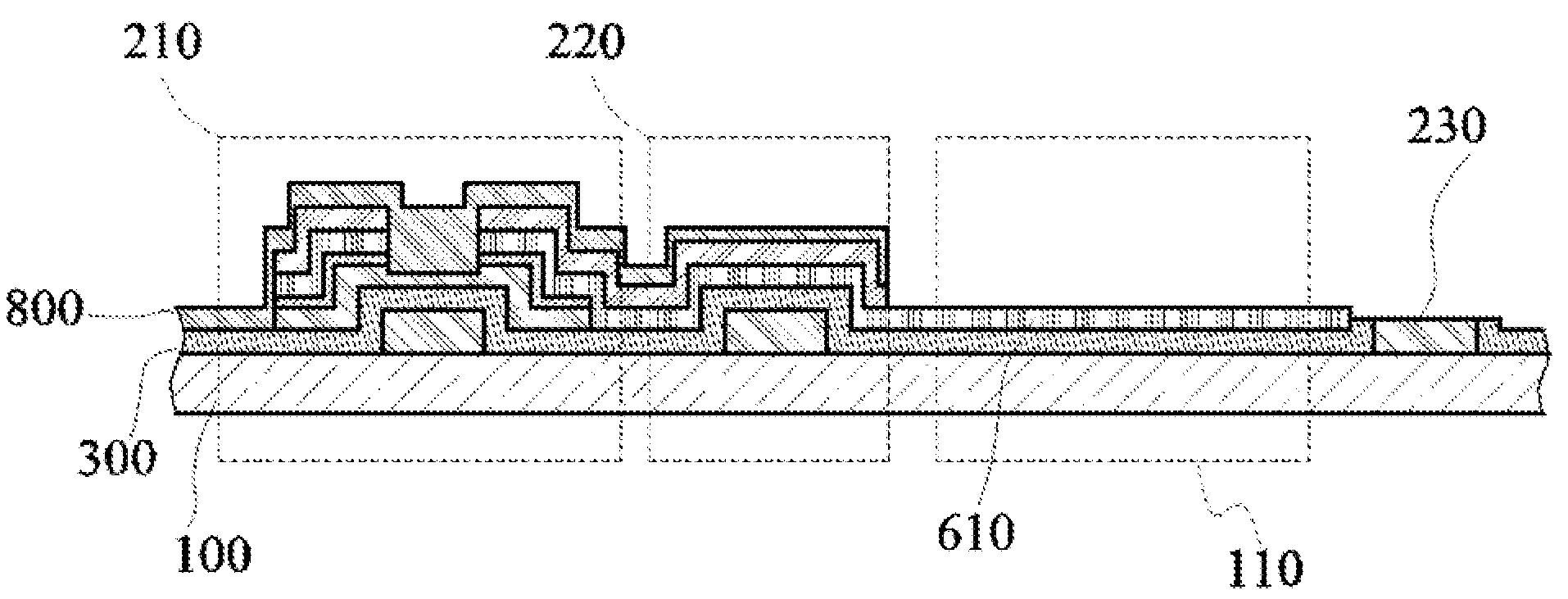
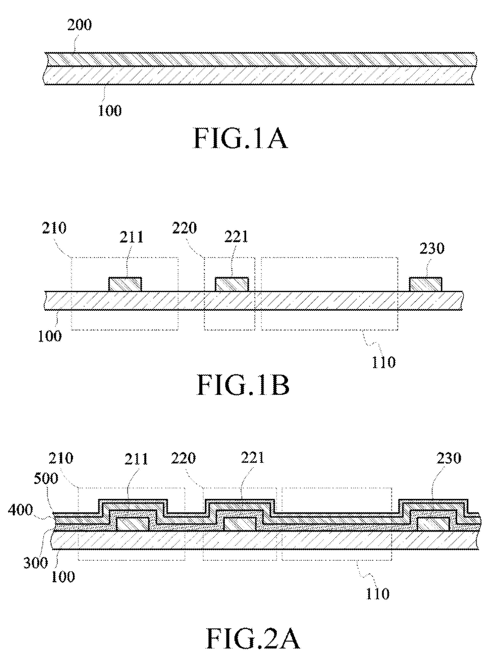
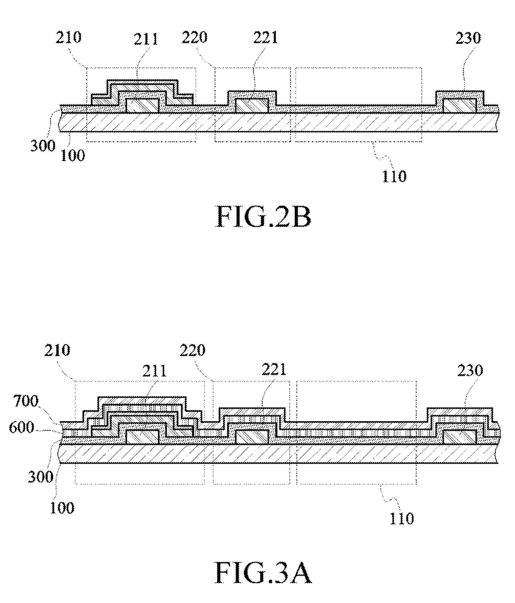
[0026]Referring to FIGS. 1A to 5, schematic sectional views of a TFT array panel of an active matrix LCD according to the present invention are shown. The fabricating flow of the TFT array panel is disclosed and the details of the processes are illustrated as follows.

[0027]As shown in FIGS. 1A and 1B, the first mask processes of the present invention are illustrated. Firstly, an insulating substrate 100 is provided, and a first metal layer 200 is formed on the insulating substrate 100 by deposition or sputtering. Then, a first mask is used to perform lithography process and etching process on the first metal layer 200, thus forming a gate electrode 211 of a TFT 210, a lower electrode 221 of a storage capacitor 220, a scan line (not shown), and a scan line pad 230 on the insulating substrate 100. Meanwhile, the profile of a pixel display region 110 is formed.

[0028]The insulating substrate 100 is made of a transparent material, such as glass, quartz, ceramic, or plastic substrates. Th...

third embodiment

[0041]Moreover, the thickness of the passivation layer 800 of the pixel display region 110 in the third embodiment can be adjusted to facilitate modulating the thickness of the liquid crystal layer in the transmissive region and the reflective region, thus achieving a preferred V-T relationship diagram (a relationship diagram between voltage and transmission rate) and a preferred V-R relationship diagram (a relationship diagram between voltage and reflectivity) and obtaining the identical phase differences to achieve preferred optical characteristics.

[0042]Referring to FIGS. 8A and 8B, schematic sectional views of the TFT array panel of an active matrix LCD according to the fourth embodiment of the present invention are shown. As shown in FIGS. 8A and 8B, the main difference between the present embodiment and the first embodiment is that before the first mask process, a first metal layer 200 and a bonding layer 900 are first sequentially deposited on the insulating substrate 100, wh...


PUM


Abstract

A thin film transistor (TFT) array panel structure and a fabrication method thereof are provided. The method includes the following steps. An insulating substrate is provided, on which a first metal layer is deposited to form a plurality of gate electrodes, a plurality of lower electrodes of storage capacitors, a plurality of scan lines, and a plurality of scan line pads with a first mask process. A TFT island region is formed with a second mask process. Drain electrodes and source electrodes of the TFT, upper electrodes of storage capacitors, pixel electrodes, data lines and data line pads are formed, and a plurality of pixel display regions is defined with a third mask process. The pattern of a passivation layer is defined with a fourth mask. A second metal layer in the pixel display region is removed by selective etching.

Description

BACKGROUND OF THE INVENTION[0001]1. Field of Invention[0002]The present invention relates to an LCD panel, and more particularly to a thin-film-transistor (TFT) array panel structure and a fabrication method thereof.[0003]2. Related Art[0004]TFTs are widely used in display pixel drive of active matrix LCDs. In general, the method of fabricating a TFT array panel of an active matrix LCD must include five mask processes. Firstly, a first metal layer is deposited on an insulating substrate (for example, a glass substrate) which serves as a display panel, and a gate electrode, a lower electrode of a storage capacitor, a scan line, and a scan line pad are formed with a first mask. Then, a gate insulator layer, an a-Si layer, and an N+ a-Si layer are sequentially deposited on the first metal layer, and the a-Si layer and N+ a-Si layer are defined as TFT islands with a second mask. Thereafter, a second metal layer is deposited on the N+ a-Si layer and the gate insulator layer. Next, a chan...

Claims


Application Information

Patent Timeline
IPC IPC(8): H01L29/04H01L21/84
CPCH01L27/1255Y10S438/982H01L27/1288
Inventor KUO, CHIEN-CHUNG
Owner WINTEK CORP
Why Eureka
Try Eureka