

Quantum Dot-Dispersed Light Emitting Device, and Manufacturing Method Thereof
a technology of light emitting devices and manufacturing methods, applied in the manufacture of electrode systems, electric discharge tubes/lamps, discharge tubes luminescnet screens, etc., to achieve the effect of large area light emitting diodes without restricting the degree of design freedom
- Summary
- Abstract
- Description
- Claims
- Application Information
AI Technical Summary
Benefits of technology
Problems solved by technology
Method used
Image

Examples
first embodiment
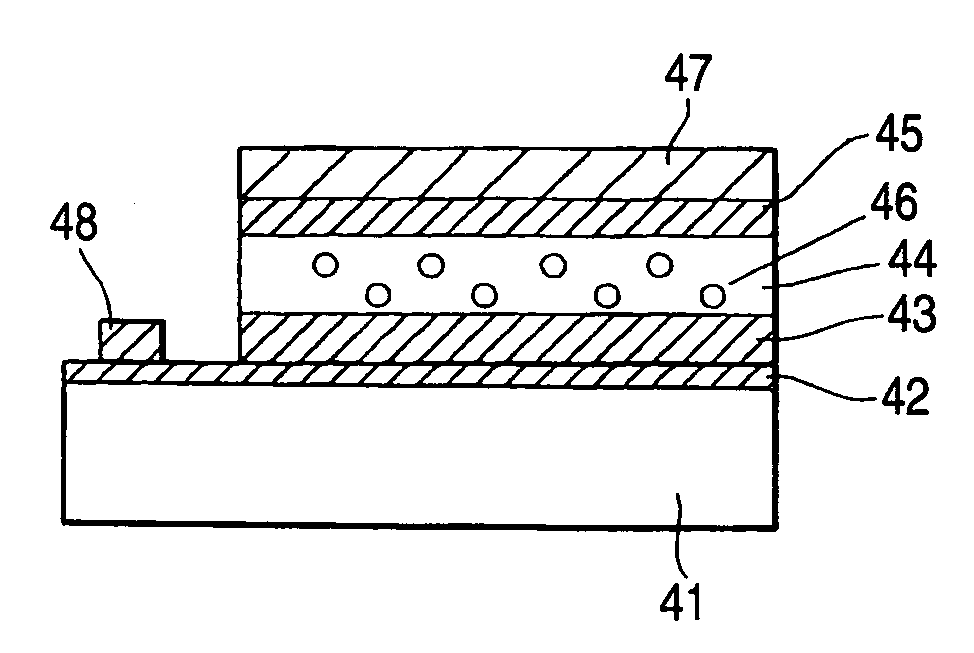
[0121](1) Structure
[0122]A light emitting diode as a quantum dot-dispersed light emitting device of the invention is, as shown in FIG. 1, characterized by being formed in such a manner that: on a substrate 11, an electron injection electrode 12, an inorganic light emitting layer 13 made of an ambipolar inorganic semiconductor material, and a hole injection electrode 14 are sequentially stacked, and the ambipolar inorganic semiconductor material includes therein nanocrystals 15 dispersed as luminescent centers, and the inorganic light emitting layer is in contact with the electron injection electrode 12 and the hole injection electrode 14 made of an amorphous phase or a polycrystalline phase, from which electrons and holes respectively flow into the nanocrystals in the inorganic light emitting layer 13 to implement efficient light emission.
[0123]Herein, the electron injection electrode and the hole injection electrode may be exchanged with each other. Namely, it is also acceptable th...
example 1
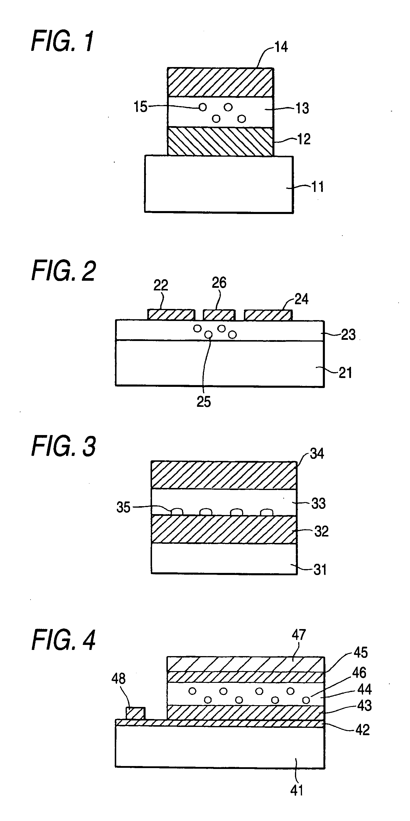
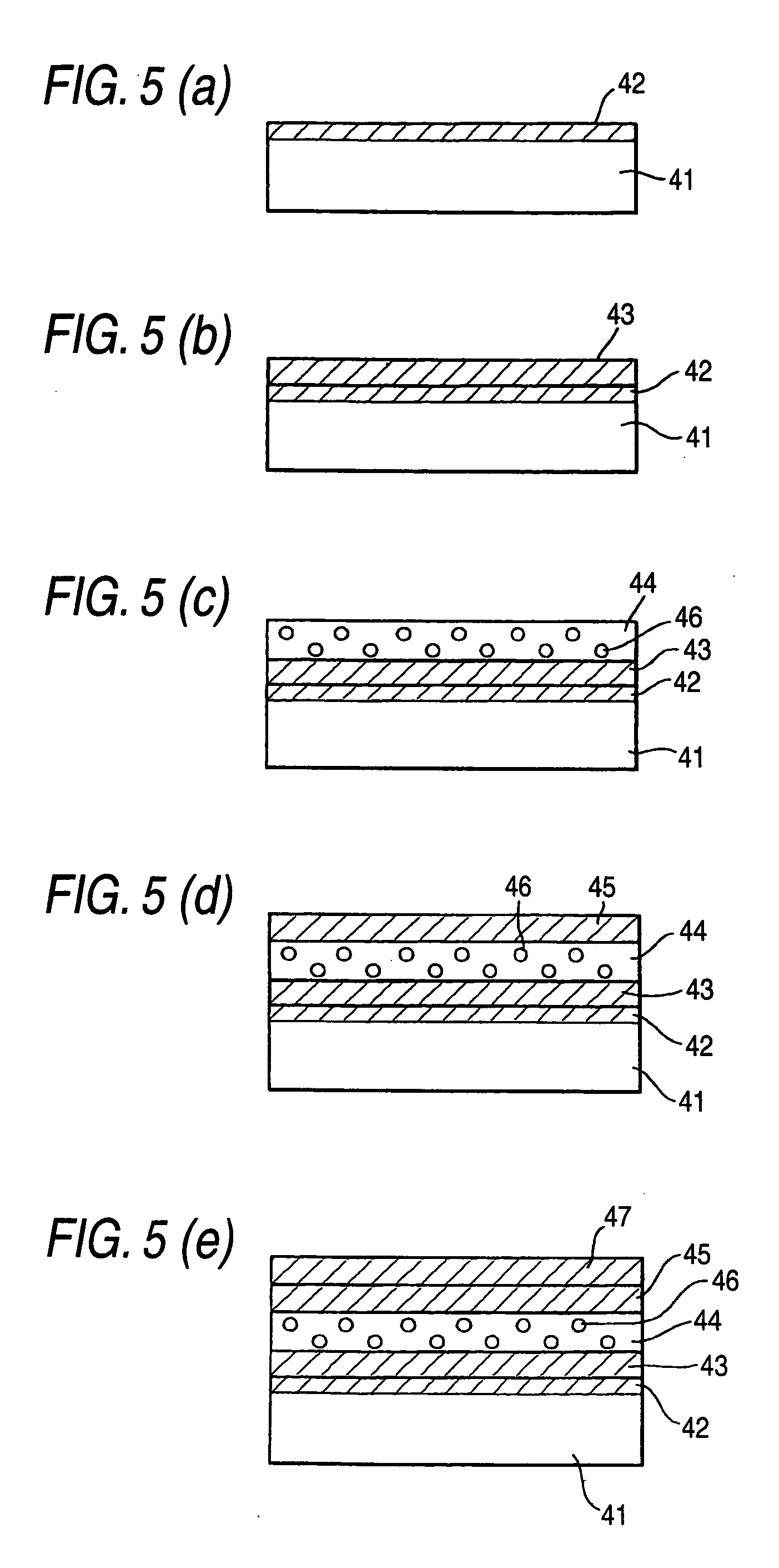
[0220]Then, an example of the invention will be described. The light emitting diode uses a glass substrate as a substrate, and may use a general glass plate. However, use of an alkali-free glass substrate for use in a liquid crystal display is preferable in that the semiconductor functions are less likely to be deteriorated.
[0221]This light emitting diode is formed in the following manner as shown in FIG. 4. On a glass substrate 41, an ITO thin film 42 (film thickness 300 nm) is formed as a transparent electrode. As a hole injection electrode 43, for example, a Cu-doped ZnSe thin film with a carrier concentration of 1×10¹⁹ / cm3 or more is deposited thereon with a film thickness of 300 nm. As a light emitting layer 44 (film thickness 30 nm), a ZnSe type amorphous ambipolar inorganic semiconductor is formed thereon. In the light emitting layer, InP nanocrystals 46 of a core shell structure with InP as the core, and with ZnSe as the shell are dispersed for the formation. Then, on the li...
examples 2 and 3
[0244]ZnSe type light emitting diodes were fabricated in the same manner as in Example 1. However, as the nanocrystal material, ZnSe-coated InP was used. As the grain sizes of InP, two sets of 2.8 nm (CV value 10%) and 4.0 nm (CV value 30%) were adopted in place of 1.8 nm (CV value 10%) in Example 1. The respective luminescent center wavelengths and spectrum half-widths when a voltage of 5 V was applied were 460 nm (half-width 30 nm), 550 nm (half-width 30 nm), and 650 nm (half-width 70 nm).
PUM
 Abstract
Description
Claims
Application Information