Optical assemblies and methods for fabrication of optical assemblies

a technology of optical assemblies and optical components, applied in the field of optical routing, can solve the problems of stray radiation absorption, cost of fabrication, and the need to control the absorption of stray radiation, and achieve the effects of high precision, effective management of wavelength isolation and stray radiation, and efficient multiplexing and demultiplexing operations

Inactive Publication Date: 2008-05-29
APPLIED MATERIALS INC
View PDF9 Cites 3 Cited by
  • Summary
  • Abstract
  • Description
  • Claims
  • Application Information

AI Technical Summary

Benefits of technology

[0009]Embodiments of the invention provide methods and structures for directing radiation. Embodiments of the invention simultaneously address multiple problems that persist with PON structures currently used. This is achieved in embodiments of the invention by using low-cost silicon fabrication methods that provide high precision to produce a structure that effectively manages wavelength isolation and stray radiation to provide efficient multiplexing and demultiplexing operations. The use of low-cost small-silicon-chip processes permits the use of small beams in tightly controlled free space instead of the use of waveguides, providing improved insertion loss and cost.
[0010]The structure makes use of grating in reflective mode for efficiency and may be produced with a low etch depth for fabrication. A focal spot may then be used that is large enough to operate the PON efficiently, but small enough to separate two beams with dispersion from the grating. The structure provides high absorption of radiation and the size of the grating coupling discriminates the wavelengths, thereby allowing the use of larger aperture detectors for improved tolerance in placement. Beams may be coupled in and out of the chip at near normal incidence for improved optical performance, especially for polarization and placement.
[0011]The use of silicon fabrication methods allows the parallel surfaces of the silicon wafers to be used to provide predictable beam angles. Standard chip-assembly techniques using low-cost passive pick-and-place tools greatly improve the fabrication efficiency over other techniques.
[0012]The result is a solution to the issue of producing PONs that uses small beams in tightly controlled free space instead of waveguides to provide improved insertion loss and cost. A wavelength separation of 60-180 nm can be well achieved with a 100-μm-diameter spacing, with about a 1-μm pitch. Merely by way of example, a focal spot diameter of 25 μm has a focus range of about 1 mm in silicon, allowing spots to be well discriminated within the geometry of the structure.

Problems solved by technology

Current implementations suffer from a number of deficiencies.
For example, persistent concerns with structures that are used exist in the isolation of the different wavelengths, the need to control the absorption of stray radiation, and the cost of fabrication.

Method used


Image

  • Optical assemblies and methods for fabrication of optical assemblies
  • Optical assemblies and methods for fabrication of optical assemblies
  • Optical assemblies and methods for fabrication of optical assemblies

Examples


Embodiment Construction

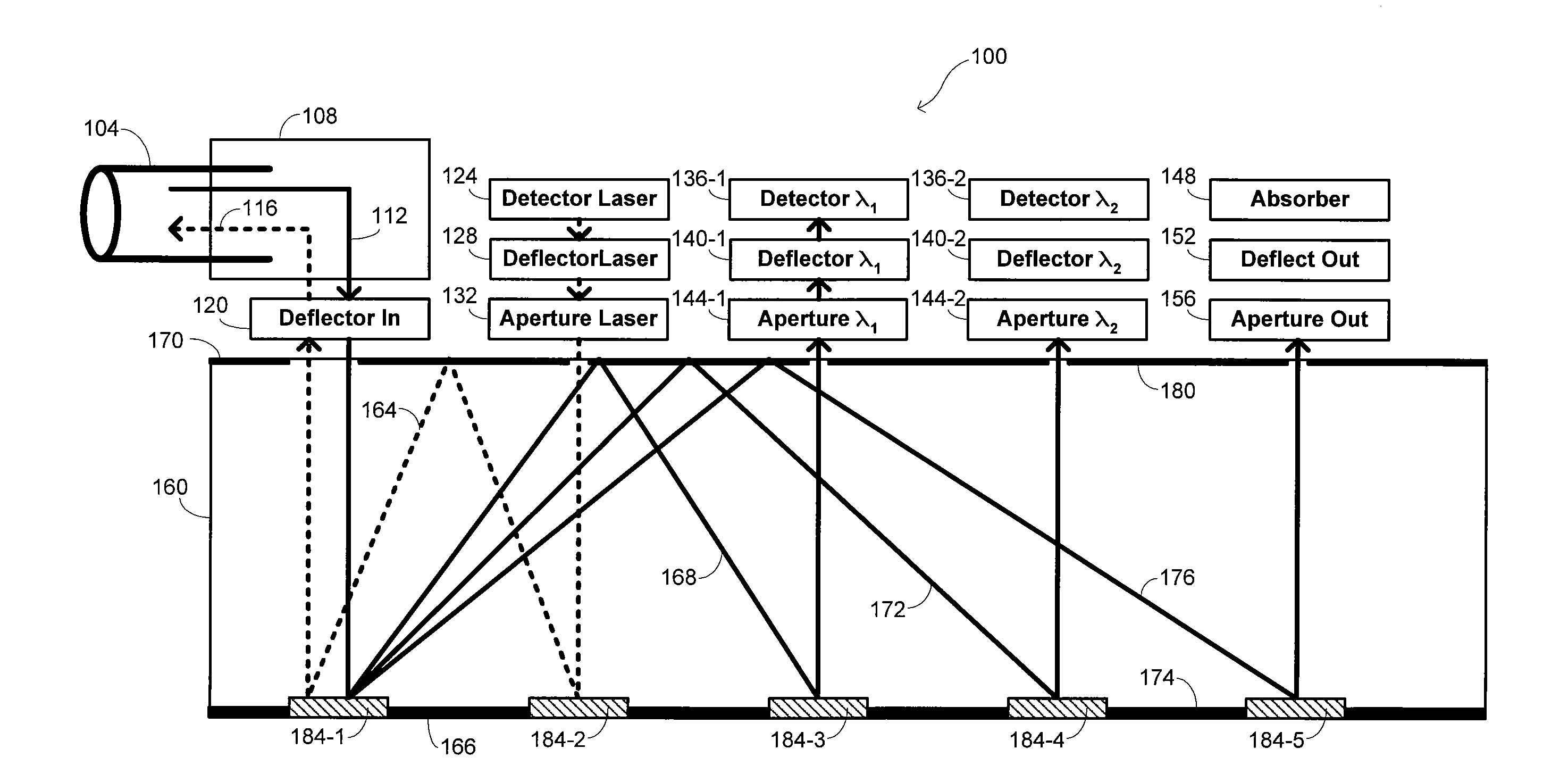
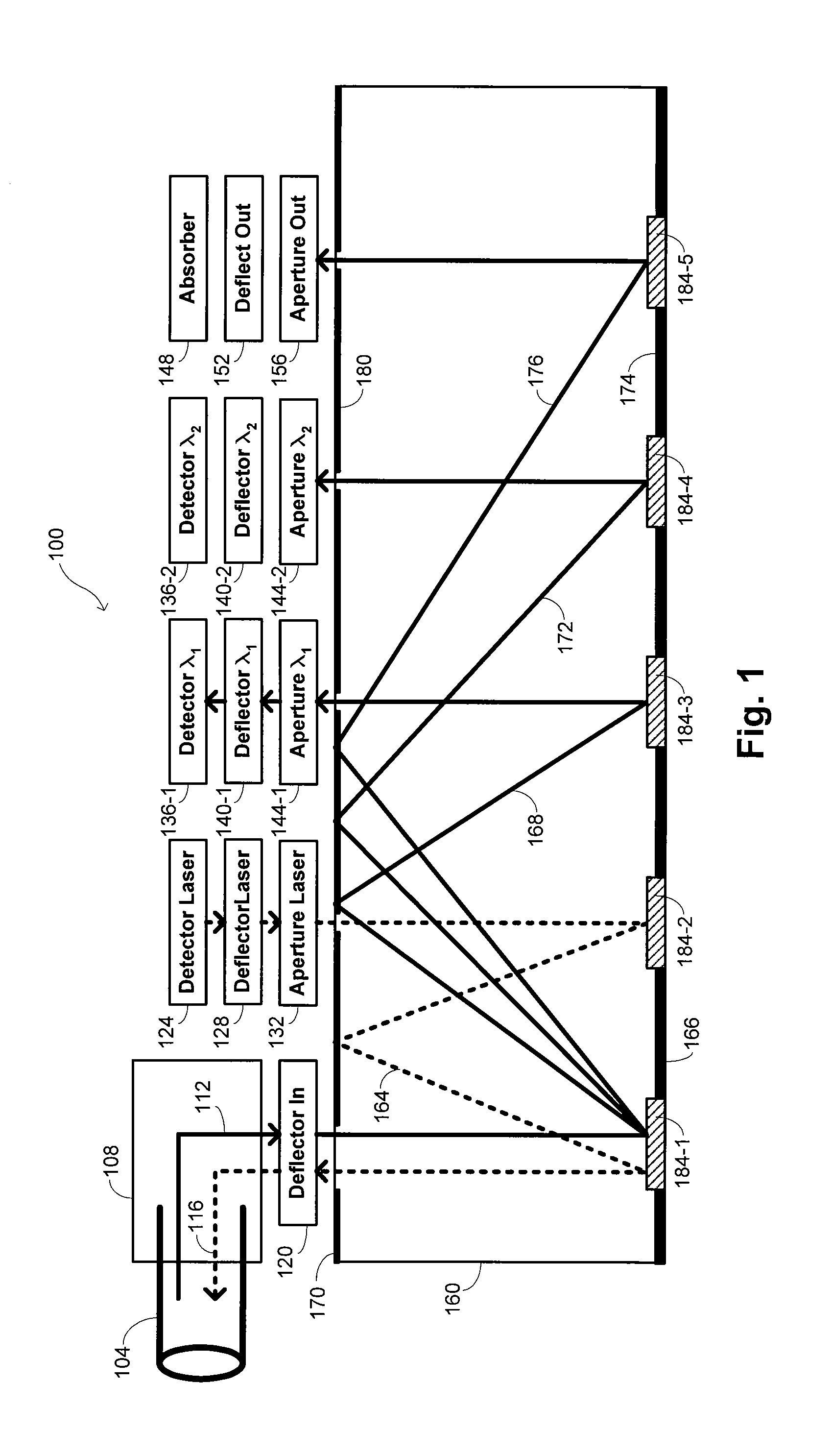
[0021]Embodiments of the invention provide optical assemblies that may be used in directing radiation. Such optical assemblies find particular application in applications in which the radiation is directed through a PON, although they may be amenable to uses in other applications also. Rather than adopt a conventional approach to providing such an optical assembly, the inventors have applied their experience with semiconductor-processing techniques to develop a structure that uses a semiconductor substrate to provide a quasi-free-space optical platform. Structural elements of an optical subassembly are fabricated using semiconductor lithographic techniques, providing a structure that may be produced at a cost significantly lower than structures produced using more conventional techniques.

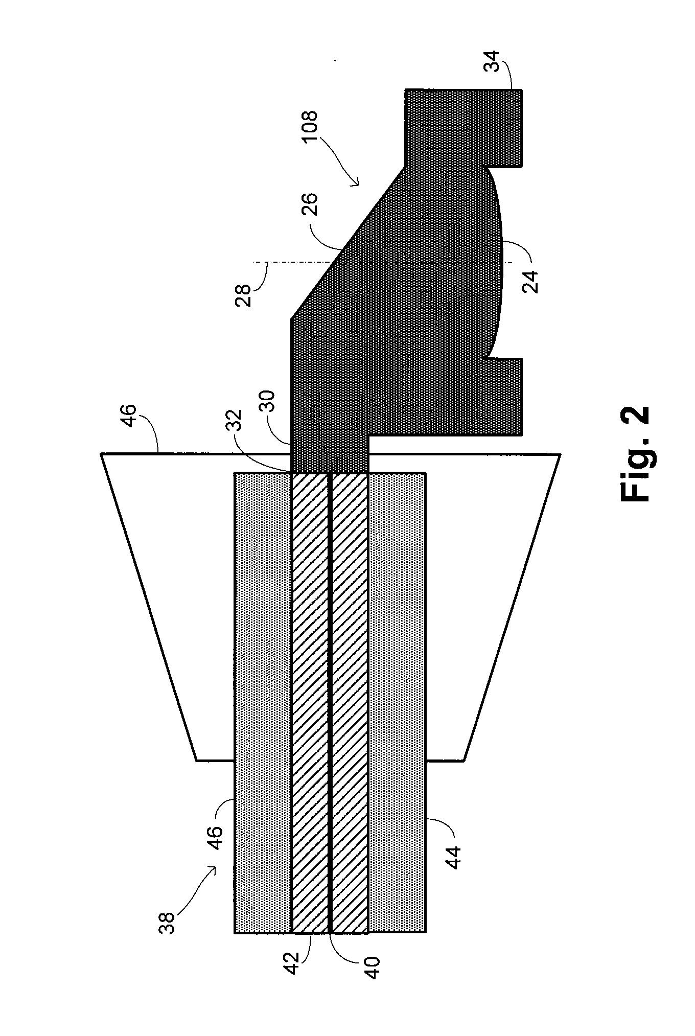
[0022]In certain embodiments, the fabrication techniques advantageously exploit the availability of pick-and-place methods for accurate fabrication of structures. The use of semiconductor-processing...


PUM


Abstract

An optical assembly is formed with a silicon substrate having a first surface and a second surface confronting the first surface. A reflective coating is formed over the first surface. Multiple diffraction gratings are formed integrally within the second surface of the silicon substrate. An optical absorber is formed over the second surface between the diffraction gratings.

Description

CROSS REFERENCE TO RELATED APPLICATION[0001]This application is a nonprovisional of, and claims the benefit of the filing date of, U.S. Prov. Pat. Appl. No. 60 / 806,348, entitled “MULTIPLEXED OPTICAL SUBASSEMBLY,” filed Jun. 30, 2006 (Attorney Docket No. AMAT 11258 USAL / NBD / OPTICS / CKIM), the entire disclosure of which is incorporated herein by reference for all purposes.[0002]This application is related to concurrently filed, commonly assigned U.S. patent application Ser. No. __ / ___,___, entitled “METHOD AND APPARATUS FOR DEMULTIPLEXING OPTICAL SIGNALS IN A PASSIVE OPTICAL NETWORK,” by Andreas Goebel et al., the entire disclosure of which is incorporated herein by reference for all purposes.BACKGROUND OF THE INVENTION[0003]This application relates generally to optical routing. More specifically, this application relates to passive optical networks.[0004]Fiber-optic telecommunications systems are currently deploying wavelength division multiplexing (“WDM”) as a mechanism for expanding...

Claims


Application Information

Patent Timeline
Patent Type & Authority Applications(United States)
IPC IPC(8): H04J14/02
CPCG02B6/2931G02B6/4246G02B6/2938
Inventor GOEBEL, ANDREASWEST, LAWRENCE C.WOJCIK, GREGORY L.
Owner APPLIED MATERIALS INC
Why Eureka
Try Eureka