Use of ion induced luminescence (IIL) as feedback control for ion implantation

a technology of ion implantation and luminescence, which is applied in the field of ion implantation for semiconductor processing systems, can solve the problems of practical monitoring methods, and achieve the effect of fast time response and accurate and fast detection times

Inactive Publication Date: 2008-06-05
AXCELIS TECHNOLOGIES
View PDF2 Cites 36 Cited by
  • Summary
  • Abstract
  • Description
  • Claims
  • Application Information

AI Technical Summary

Benefits of technology

[0012]Another aspect of the present invention is that the signal can have a faster time response, than current monitoring systems, since the ion induced luminescence response time is of the order of 10−12-10−8 seconds for most inorganic materials and of the order of 10−9-10−7 seconds for organic materials. High gain, low-noise pho...

Problems solved by technology

Directly measuring beam current,.for example while the ion beam is directly on the wafer is nearly impossible by conventional means and only indirect beam current monitoring methods are practical.
However, there are several problems associated ...

Method used


Image

  • Use of ion induced luminescence (IIL) as feedback control for ion implantation
  • Use of ion induced luminescence (IIL) as feedback control for ion implantation
  • Use of ion induced luminescence (IIL) as feedback control for ion implantation

Examples


Embodiment Construction

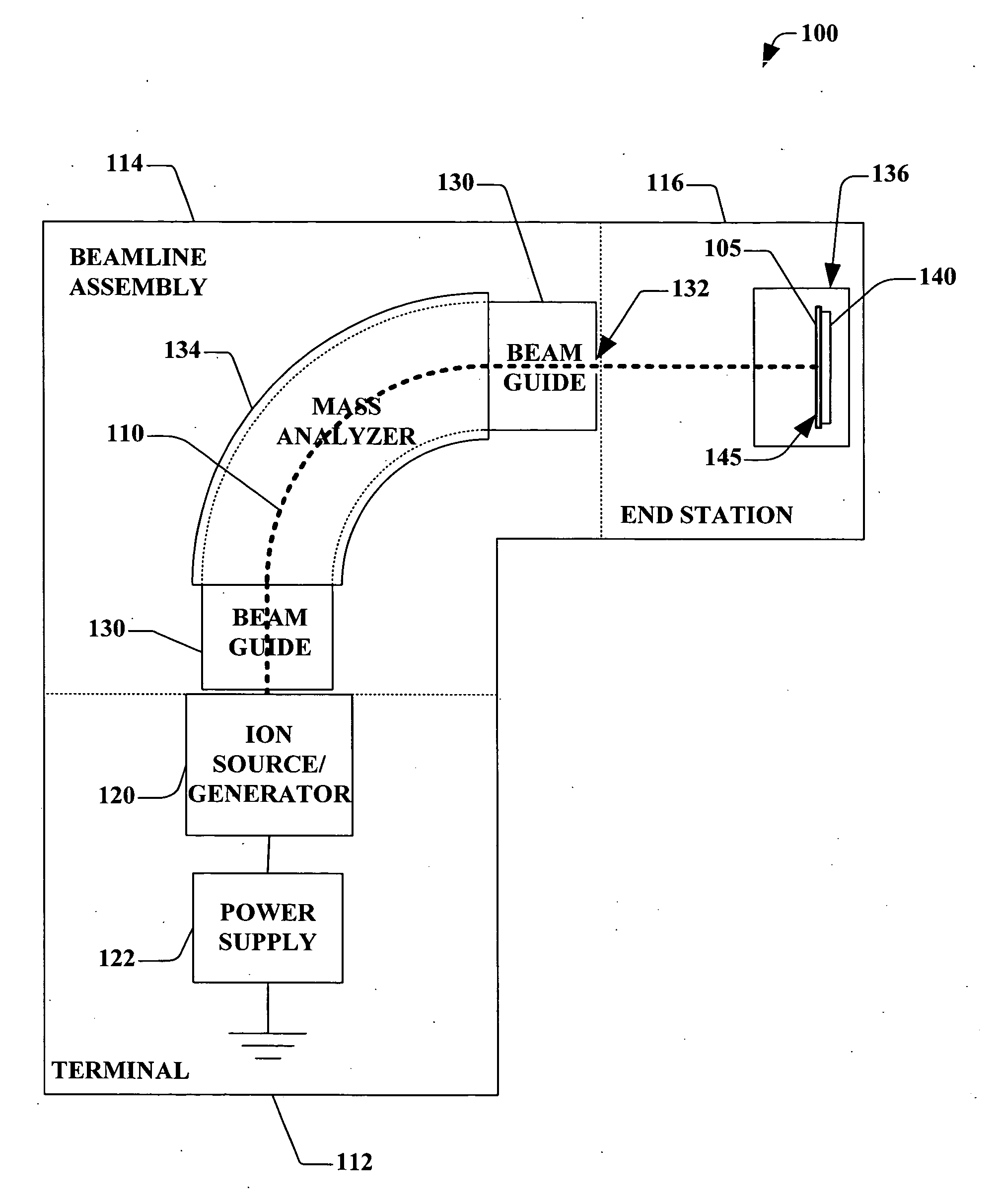
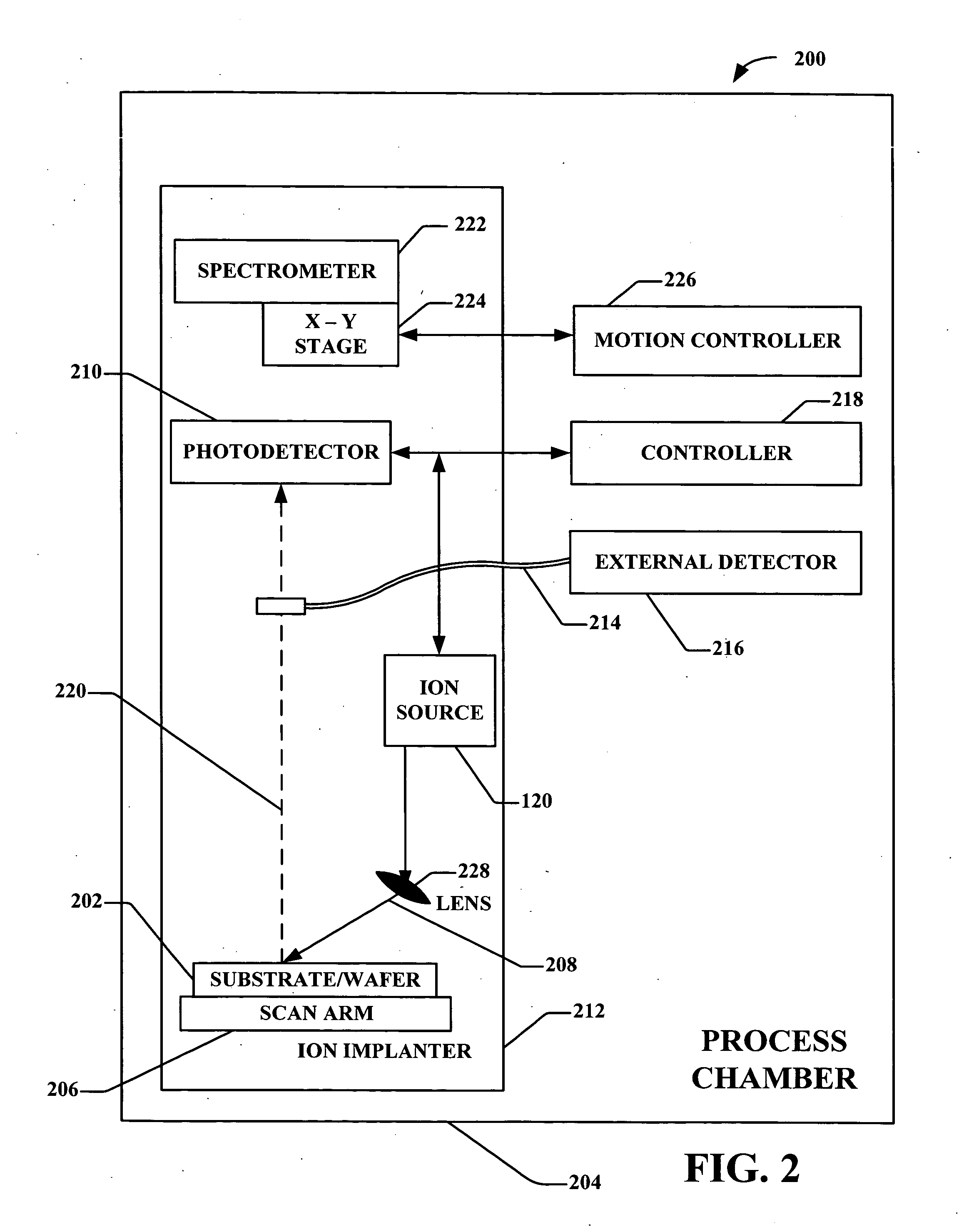
[0024]The present invention is directed generally towards a system and method for employing ion induced luminescence when manufacturing or processing semiconductors using an ion implantation system. More particularly, the system and method provides an optimized approach based on one or more performance criteria associated with the ion source implantation system. Accordingly, the present invention will now be described with reference to the drawings, wherein like reference numerals are used to refer to like elements throughout. It should be understood that the description of these aspects are merely illustrative and that they should not be taken in a limiting sense. In the following description, for purposes of explanation, numerous specific details are set forth in order to provide a thorough understanding of the present invention. It will be evident to one of ordinary skill in the art, however, that the present invention may be practiced without these specific details.

[0025]Referri...


PUM


Abstract

An ion implantation system utilizing detected ion induced luminescence as feedback control that comprises, a wafer, a spectrometer, a photodetector, an ion source generator, wherein the ion source generator is configured to implant the wafer with ions, and the photodetector is configured to detect ion induced luminescence both on and off the wafer.

Description

FIELD OF THE INVENTION[0001]The present invention relates generally to ion implantation for semiconductor processing systems, and more specifically to a method for optimizing ion implantation of a semiconductor substrate by employing luminescence as feedback control.BACKGROUND OF THE INVENTION[0002]The semi-conductor industry employs ion implantation in the manufacture and processing of very large scale integration (VLSI) microprocessors. Ion implantation is a process by which dopants are added to a semiconductor wafer by impacting energized and accelerated charged atoms or molecules (positive or negative ions) against semiconductor substrates. One of the objectives of ion implantation is to introduce a desired atomic species uniformly into a target material, the semiconductor wafer.[0003]Measuring and / or attaining precise dose uniformity over a wafer surface is typically accomplished by scanning a beam of ions across the wafer surface. To ensure the surface of the wafer is “painted...

Claims


Application Information

Patent Timeline
IPC IPC(8): G01J5/00G01J1/32
CPCG01N23/2255G01N2223/6116H01J37/244H01J37/304H01J2237/24514H01J2237/2443H01J2237/2445H01J2237/24507H01J37/3171
Inventor BERRY, IVAN L.
Owner AXCELIS TECHNOLOGIES
Why Eureka
Try Eureka