Schottky barrier nanowire field effect transistor and method for fabricating the same

a field effect transistor and nanowire technology, applied in the field of semiconductor devices, can solve the problems that conventional semiconductor devices are reaching their scaling limits, and achieve the effects of ensuring thermal stability, excellent gate controllability, and convenient fabrication

Inactive Publication Date: 2008-06-05
ELECTRONICS & TELECOMM RES INST
View PDF6 Cites 147 Cited by
  • Summary
  • Abstract
  • Description
  • Claims
  • Application Information

AI Technical Summary

Benefits of technology

[0010]Another embodiment of the present invention is directed to provide a Schottky barrier nanowire FET which is easy to fabricate and can ensure thermal stability and have excellent gate controllability, and a method for fabricating the same.

Problems solved by technology

As the integration density of semiconductor devices increases, conventional semiconductor devices are reaching their scaling limits.

Method used


Image

  • Schottky barrier nanowire field effect transistor and method for fabricating the same
  • Schottky barrier nanowire field effect transistor and method for fabricating the same
  • Schottky barrier nanowire field effect transistor and method for fabricating the same

Examples


Embodiment Construction

[0026]The advantages, features and aspects of the invention will become apparent from the following description of the embodiments with reference to the accompanying drawings, which is set forth hereinafter. In the drawings, the dimensions of layers and regions are exaggerated for clarity of illustration. It will also be understood that when a layer (or film) is referred to as being “on“another layer or substrate, it can be directly on the other layer or substrate, or intervening layers may also be present. Like reference numerals refer to like elements throughout the drawings.

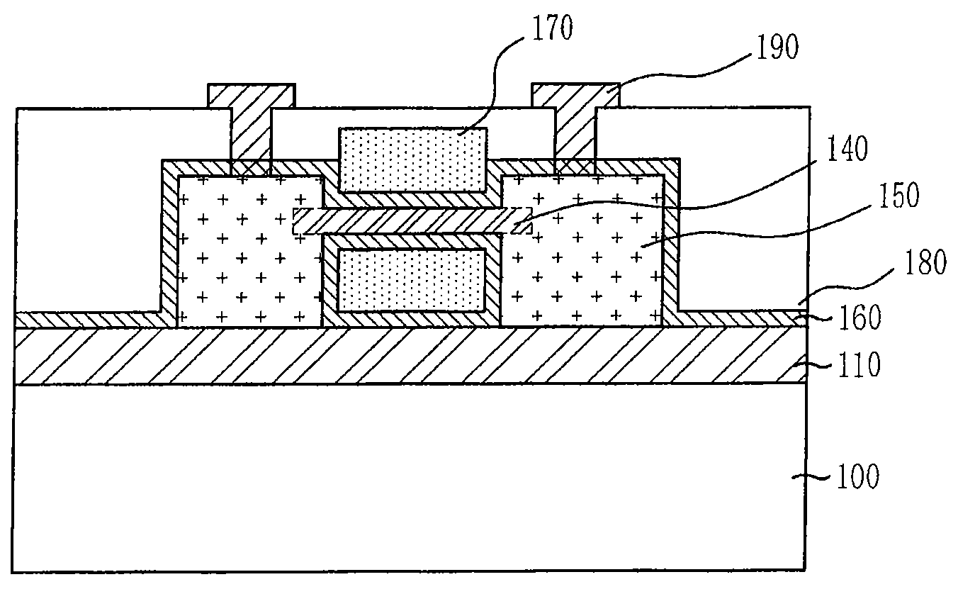
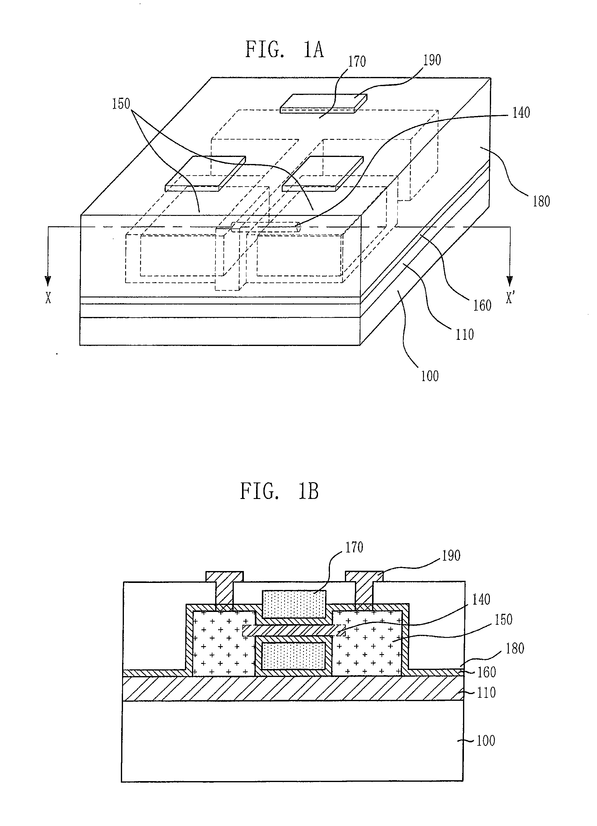
[0027]FIG. 1A is a perspective view of a Schottky barrier nanowire FET in accordance with an embodiment of the present invention, and FIG. 1B is a cross-sectional view taken along line X-X′ of FIG. 1A.

[0028]Referring to FIGS. 1A and 1B, the Schottky barrier nanowire FET includes a substrate 100, a channel 140 suspended over the substrate 100 and formed of a nanowire, source / drain electrodes 150 electrically co...


PUM

PropertyMeasurementUnit
diameteraaaaaaaaaa
temperatureaaaaaaaaaa

Abstract

Provided is a Schottky barrier nanowire field effect transistor, which has source / drain electrodes formed of metal silicide and a channel formed of a nanowire, and a method for fabricating the same. The Schottky barrier nanowire field effect transistor includes: a channel suspended over a substrate and including a nanowire; metal silicide source / drain electrodes electrically connected to both ends of the channel over the substrate; a gate electrode disposed to surround the channel; and a gate insulation layer disposed between the channel and the gate electrode.

Description

CROSS-REFERENCE(S) TO RELATED APPLICATIONS[0001]The present invention claims priority of Korean Patent Application Nos. 10-2006-0121276 and 10-2007-0100558, filed on Dec. 4, 2006, and Oct. 5, 2007, respectively, which are incorporated herein by reference.BACKGROUND OF THE INVENTION[0002]1. Field of the Invention[0003]The present invention relates to a semiconductor device and a method for fabricating the same; and, more particularly, to a Schottky barrier nanowire field effect transistor, which has source / drain electrodes formed of metal silicide and a channel formed of a nanowire, and a method for fabricating the same.[0004]This work was supported by the IT R&D program of MIC / IITA [2005-S-104-02, “High-tech semiconductor nano device for information communication”].[0005]2. Description of Related Art[0006]As the integration density of semiconductor devices increases, conventional semiconductor devices are reaching their scaling limits. So far, many methods of scaling the device have...

Claims


Application Information

Patent Timeline
Patent Type & Authority Applications(United States)
IPC IPC(8): H01L21/338H01L29/00
CPCB82Y10/00H01L29/0665H01L29/0673H01L29/42392H01L29/458H01L51/0508H01L29/7839H01L29/78681H01L29/7869H01L29/78696H01L51/0048H01L29/775H10K85/221H10K10/46
Inventor JUN, MYUNGSIMJANG, MOON-GYUKIM, YARK-YEONCHOI, CHEL-JONGKIM, TAEYOUBLEE, SEONGJAE
Owner ELECTRONICS & TELECOMM RES INST
Why Eureka
Try Eureka