

Semiconductor Device and Method of Manufacturing Same
- Summary
- Abstract
- Description
- Claims
- Application Information
AI Technical Summary
Benefits of technology
Problems solved by technology
Method used
Image

Examples
embodiment mode 1
[0044]In this embodiment mode, a structure of a semiconductor device which can suppress leak current caused by a reduction in coverage by a gate insulating layer at an end portion of a semiconductor layer will be described.
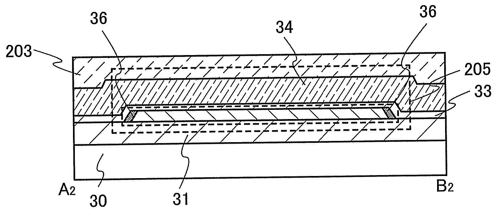
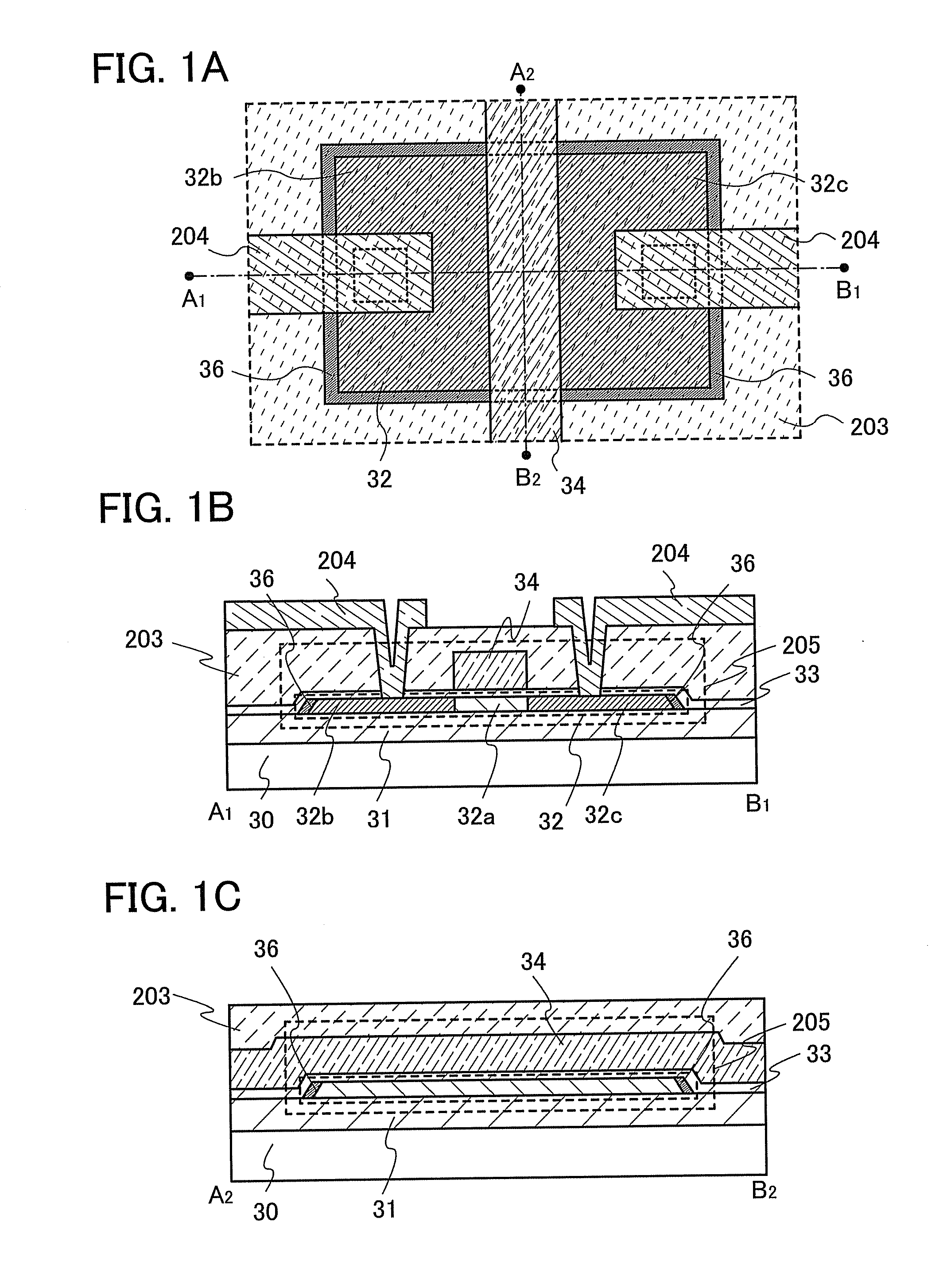
[0045]FIGS. 1A to 1C are a top view and cross sections which show a main structure of a semiconductor device of the invention. FIG. 1A is a top view which shows main parts of a thin film transistor. FIG. 1B shows a cross section taken along the broken line joining A1 and B1 in FIG. 1A. FIG. 1C shows a cross section taken along the broken line joining A2 and B2 in FIG. 1A.
[0046]A semiconductor device described in this embodiment mode includes a thin film transistor 205 having an island-shaped semiconductor layer 32 which is provided over a substrate 30 with an insulating layer 31 interposed therebetween and a conductive layer 34 which serves as a gate electrode which is provided over the semiconductor layer 32 with a gate insulating layer 33 interposed therebetween...
embodiment mode 2
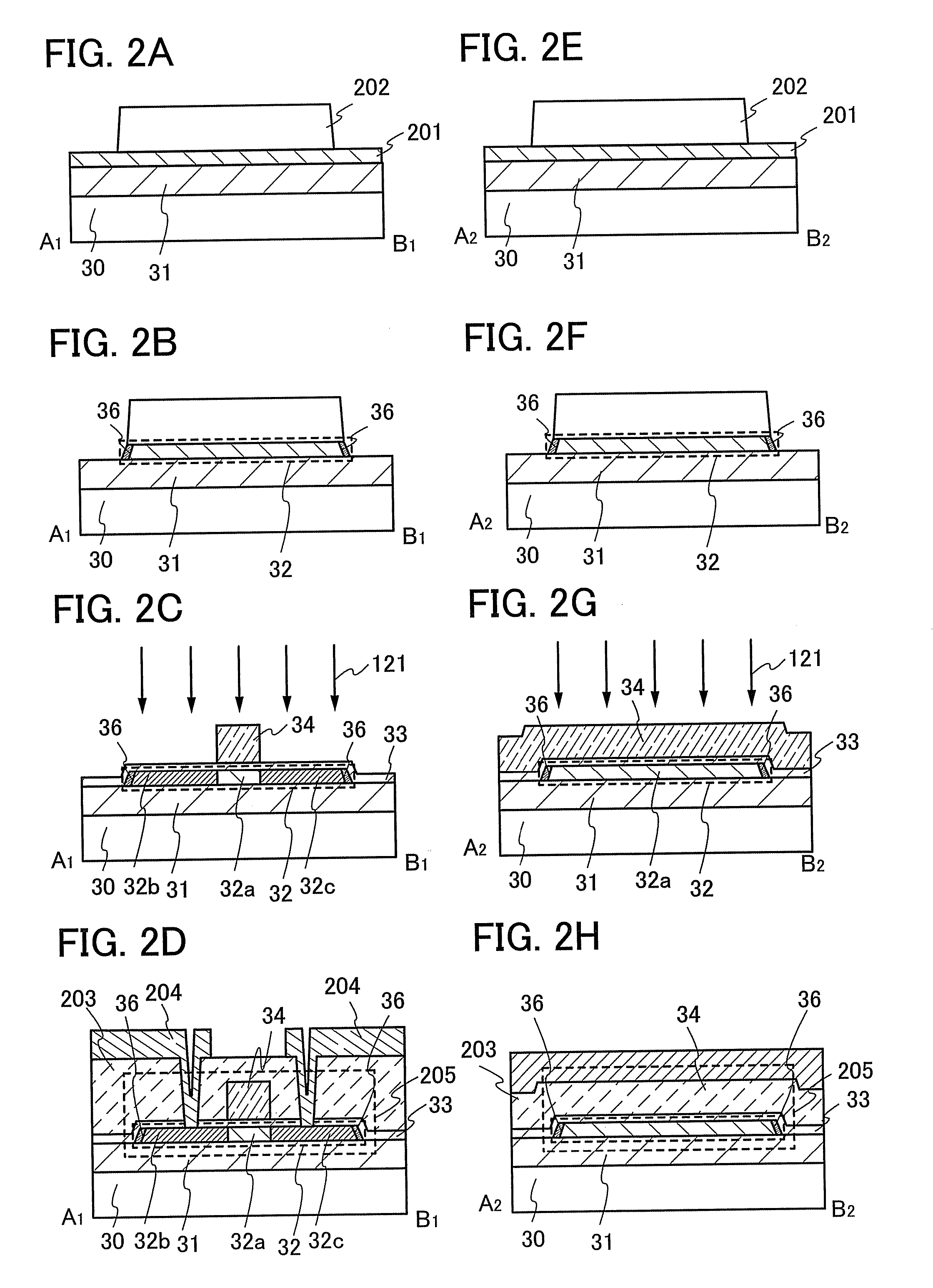
[0057]In this embodiment mode, an example of a method of manufacturing the semiconductor device shown in FIGS. 1A to 1C will be described with reference to the drawings. Note that in this embodiment mode, manufacturing process steps which relate to the cross section taken along the broken line joining A1 and B1 in FIG. 1A are described with reference to FIGS. 2A to 2D, and manufacturing process steps which relate to the cross section taken along the broken line joining A2 and B2 in FIG. 1A are described with reference to FIGS. 2E to 2H.
[0058]First, the insulating layer 31 is formed over the substrate 30 (FIGS. 2A and 2E).
[0059]As the substrate 30, a glass substrate, a quartz substrate, a metal substrate (for example, a stainless steel substrate or the like), a ceramic substrate, a semiconductor substrate, such as a Si substrate, or the like can be used. Alternatively, a plastic substrate formed of polyethylene terephthalate (PET), polyethylene naphthalate (PEN), polyether sulfone (P...
embodiment mode 3
[0091]In this embodiment mode, a method of manufacturing the semiconductor device shown in FIGS. 1A to 1C which differs to that described in Embodiment Mode 2 will be described. In this embodiment mode, manufacturing process steps which relate to the cross section taken along the broken line joining A1 and B1 in FIG. 1A are explained with reference to FIGS. 3A and 3B, and manufacturing process steps which relate to the cross section along the broken line joining A2 and B2 in FIG. 1A are explained with reference to FIGS. 3C and 3D.
[0092]First, as in Embodiment Mode 2, the insulating layer 31 is formed over the substrate 30, the semiconductor layer 201 is formed over the insulating layer 31, and the resist 202 is formed over the semiconductor layer 201 (FIGS. 3A and 3C).
[0093]Next, the island-shaped semiconductor layer 32 is formed by etching the semiconductor layer 201 using the resist 202 as a mask (FIGS. 3B and 3D).
[0094]Subsequently, by removing the resist 202, then oxidizing the ...
PUM
 Abstract
Description
Claims
Application Information