Articles and assembly for magnetically directed self assembly and methods of manufacture

Inactive Publication Date: 2008-06-12
GENERAL ELECTRIC CO
View PDF13 Cites 24 Cited by
  • Summary
  • Abstract
  • Description
  • Claims
  • Application Information

AI Technical Summary

Benefits of technology

[0009]One aspect of the present invention resides in a functional block for assembly. The functional block includes at least one element and a magnetic film attached to the element and having a magnetic remanence (MR/MS) of less than about 0.2, having a coercive field (Hc) of less than about 100 Oersteds (100 Oe) and h

Problems solved by technology

A key limitation of the pick and place approach is that the components must be serially placed on the PCB.
Therefore, as the number of components to be assembled increases, the manufacturing cost increases to the point where costs become prohibitive.
In addition, as the component size decreases, it becomes increasingly difficult to manipulate and position the components using robotics.
Accordingly, this technique is ill-suited for the manufacture of low density, distributed electronics, such as flat panel displays or digital x-ray detectors.
Although a-Si TFTs have been successfully fabricated over large areas (e.g. liquid crystal displays), the transistor performance is relatively low and therefore limited to simple switches.
In addition, with this process, the unit cost of a large area electronic circuit necessarily scales with the size of the circuit.
While TFTs formed using these higher mobility materials have been shown to be useful for small-scale circuits, their transistor characteristics are inferior to single crystal transistors, and thus circuits made from these materials are inherently inferior to their single crystal counterparts.
A drawback of both magnetic techniques disclosed in Schatz is that the components will tend to agglomerate in solution due to the high remanent magnetization typical of high permeability magnetic materials.
Schatz does not recognize or address this issue.
Nor does Schatz teach or suggest a method for producing magnetic films that overcome this issue.
This technique suffers from several drawbacks, including severe limitatio

Method used


Image

  • Articles and assembly for magnetically directed self assembly and methods of manufacture
  • Articles and assembly for magnetically directed self assembly and methods of manufacture
  • Articles and assembly for magnetically directed self assembly and methods of manufacture

Examples


example

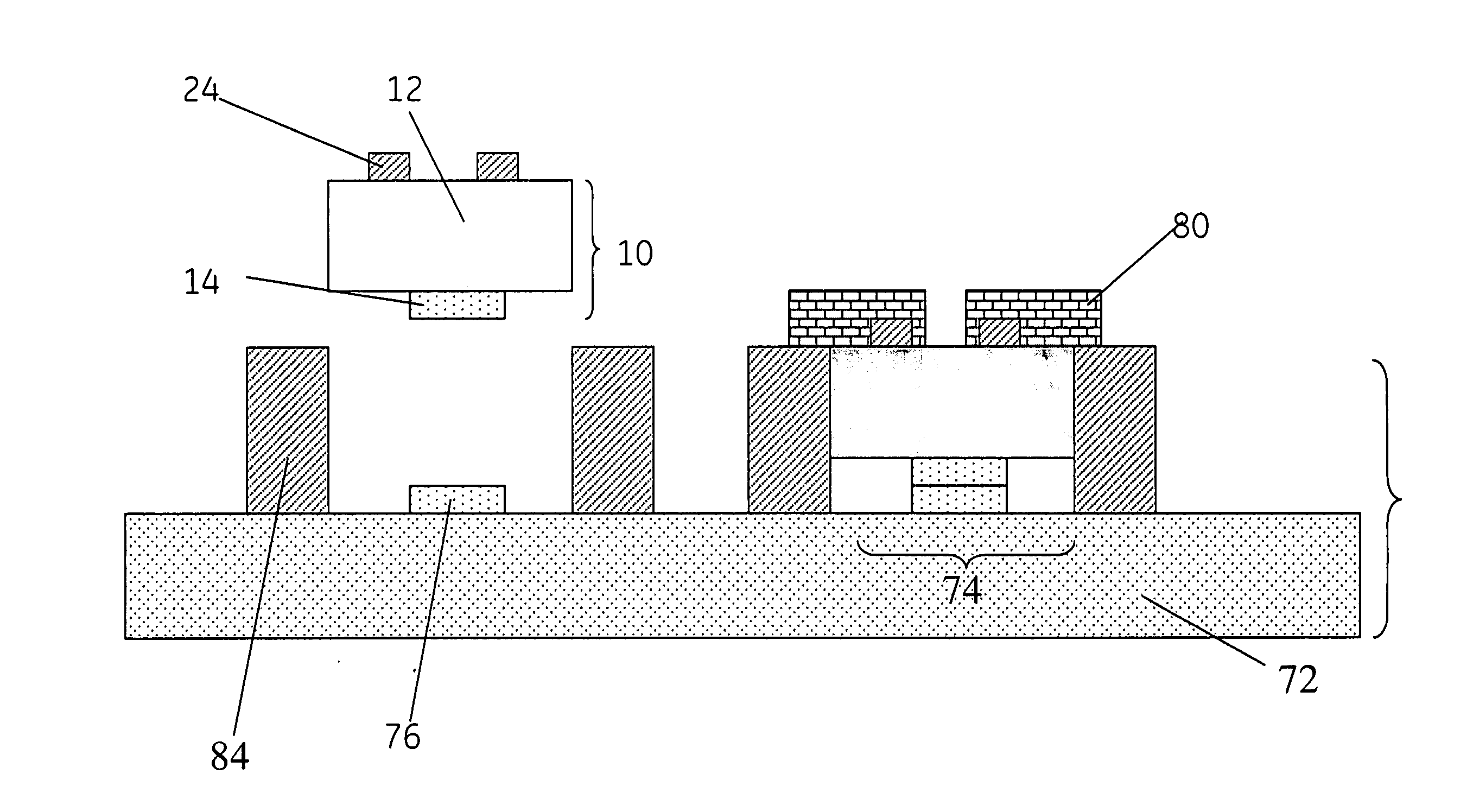
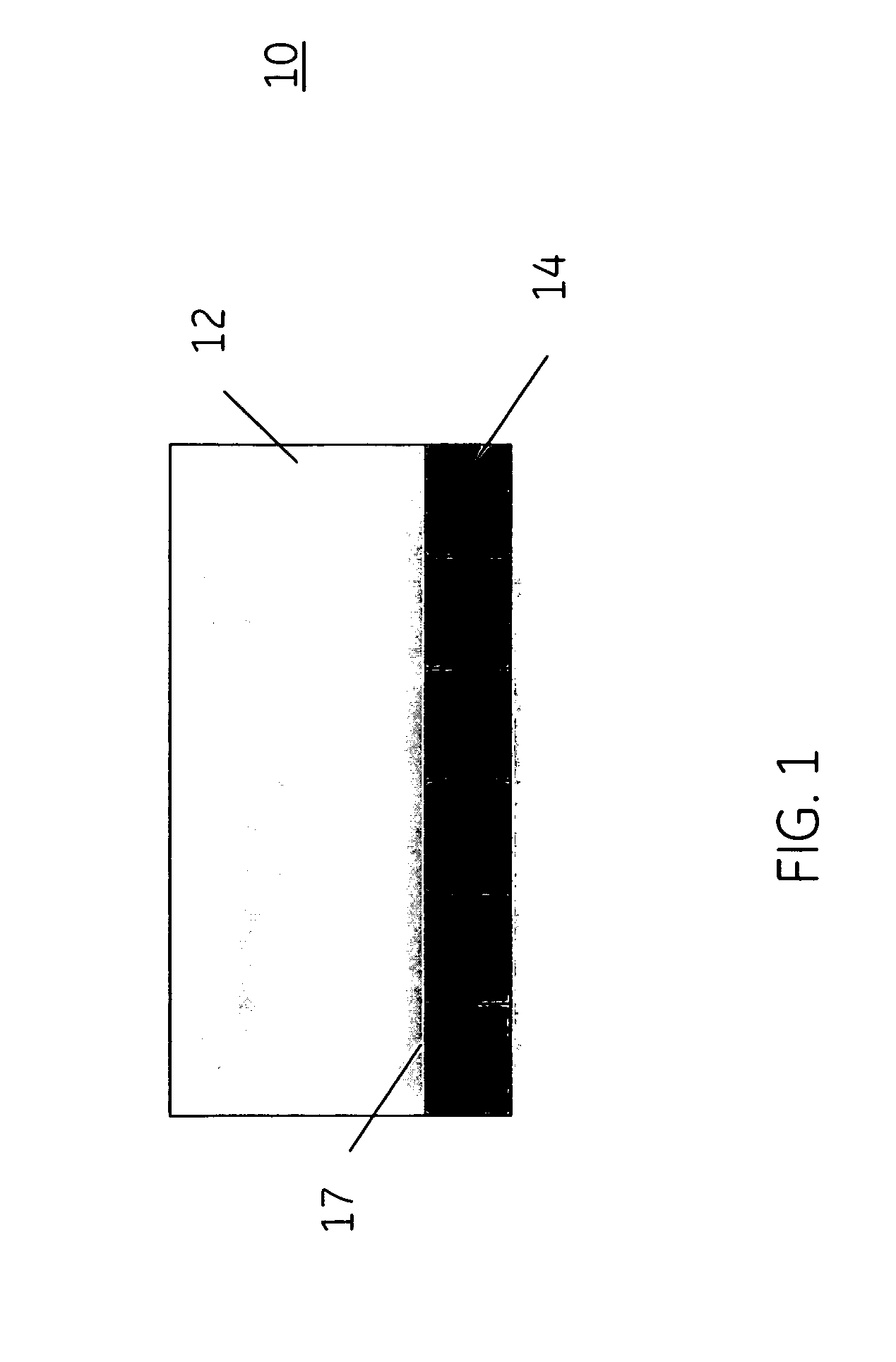
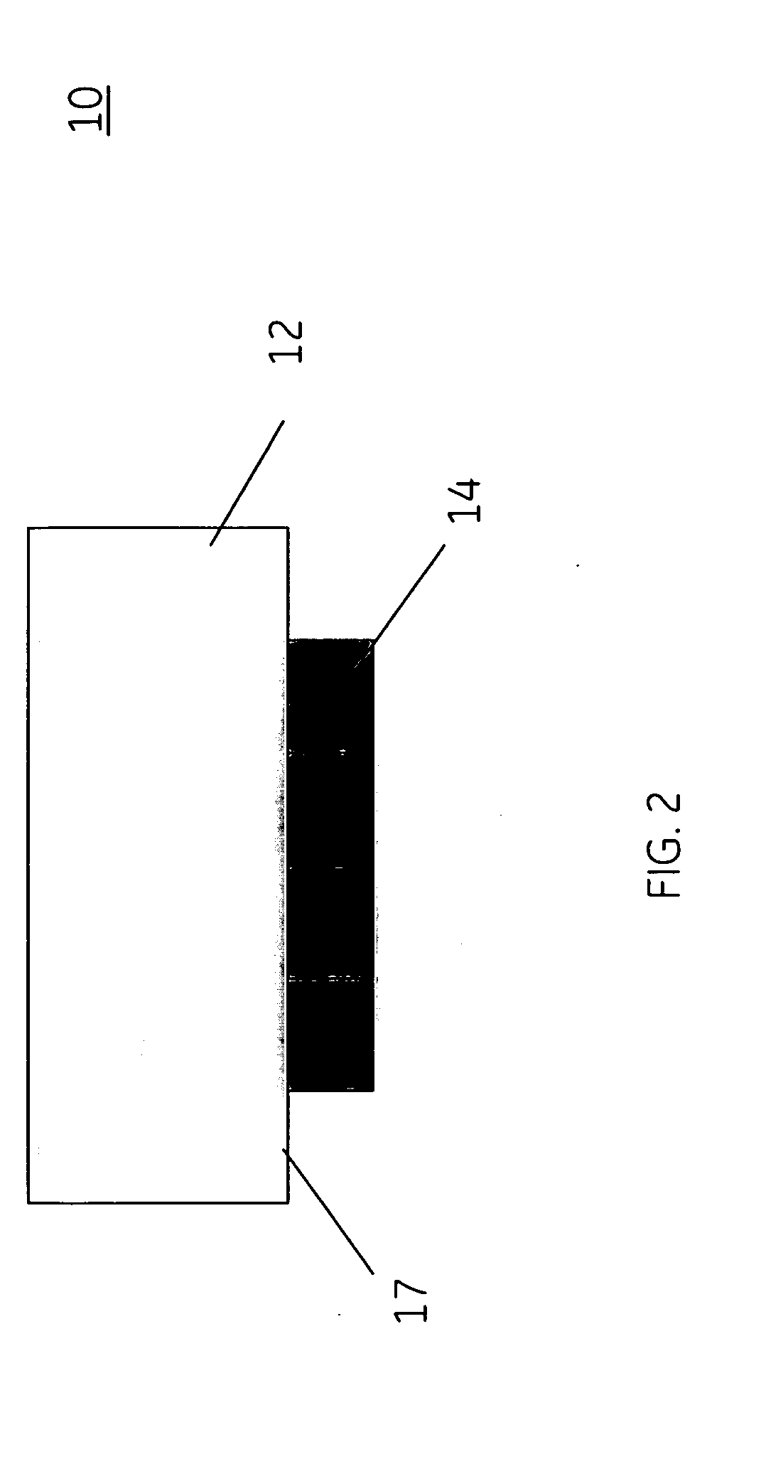
[0038]The magnetic film 14 may be fabricated from a variety of different materials using a variety of different techniques. In one non-limiting example illustrated by FIG. 11, the magnetic film 14 comprises superparamagnetic nanoparticles 34 embedded in a polymer binder 36. Non-limiting examples of superparamagnetic nanoparticles 34 include Fe3O4, γ-Fe2O3, Ni80Fe20, NiFe2O4, MnFe2O4, MnZn ferrite, NiZn ferrite, Ni, Fe and combinations thereof. As is known in the art, certain magnetic nanoparticles prone to oxidation may be coated with a barrier layer to reduce oxidation. Non-limiting examples of barrier layers (not shown) include Au, Ag, SiO2, Al2O3, TiO2 and Si3N4. Non-limiting examples of polymer binders 36 include thermosetting compounds such as PI-2555 polyimide resin from HD Microsystems and thermoplastics such as nylon. The magnetic film 14 may also contain additional dispersants to reduce particle agglomeration and / or adhesion promoters as is known in the art. The compound ca...


PUM

PropertyMeasurementUnit
Auxiliary magnetic fieldaaaaaaaaaa
Magnetic fieldaaaaaaaaaa
Adhesivityaaaaaaaaaa

Abstract

A functional block for assembly includes at least one element and a magnetic film attached to the element and having a magnetic remanence (MR/MS) of less than about 0.2, having a coercive field (Hc) of less than about 100 Oersteds (100 Oe) and having a permeability (μ) of greater than about two (2). At least one element is selected from the group consisting of a semiconductor device, a passive element, a photonic bandgap element, a luminescent material, a sensor, a micro-electrical mechanical system (MEMS), an energy harvesting device and combinations thereof. An article for assembly includes a substrate and a patterned magnetic film disposed on the substrate and defining at least one receptor site. The patterned magnetic film is magnetized primarily in a longitudinal direction and is characterized by a BH product of greater than about 1 megaGauss Oe.

Description

BACKGROUND[0001]The invention relates generally to the assembly of components onto a surface, and more particularly, to the assembly of building blocks onto a substrate for electronic circuit fabrication, sensors, energy conversion, photonics and other applications.[0002]There is a concerted effort to develop large area, high performance electronics for applications such as medical imaging, nondestructive testing, industrial inspection, security, displays, lighting and photovoltaics, among others. Two approaches are typically employed. For systems involving large numbers of active elements (for example, transistors) clustered at a relatively small number of locations, a “pick and place” technique is typically employed, for which the active elements are fabricated, for example using single crystal semiconductor wafers, and singulated (separated) into relatively large components (for example, on the order of 5 mm) comprising multiple active elements. The components are sequentially pl...

Claims


Application Information

Patent Timeline
IPC IPC(8): H01L29/82B32B3/00B05D5/12
CPCH01F1/083H01F1/113H01F1/26H01F1/37H01L24/81H01L24/83H01L24/93H01L24/95H01L25/50H01L2224/32014H01L2224/81121H01L2224/81136H01L2224/81801H01L2224/83121H01L2224/83136H01L2224/83143H01L2224/83191H01L2224/83194H01L2224/83801H01L2224/95144H01L2924/01002H01L2924/01005H01L2924/01013H01L2924/01015H01L2924/01025H01L2924/01027H01L2924/01029H01L2924/0103H01L2924/01038H01L2924/01042H01L2924/01046H01L2924/01047H01L2924/0105H01L2924/01056H01L2924/01064H01L2924/01073H01L2924/01074H01L2924/01078H01L2924/01079H01L2924/01082H01L2924/10329H01L2924/13055H01L2924/13091H01L2924/19041H01L2924/19042H01L2924/19043H01L24/32H01L2924/01006H01L2924/01024H01L2924/01033H01L2924/01065H01L2924/014H01L2924/0132H01L2924/0133H01L2924/0134H01L2224/95085H01L2224/8113H01L2224/81132H01L2924/1461H01L2924/1305Y10T428/24917H01L2924/01026H01L2924/01014H01L2924/01032H01L2924/01049H01L2924/01028H01L2924/01031H01L2924/00H01L2224/32055H01L2924/00015
Inventor HUBER, WILLIAM HULLINGERJOHNSON, FRANCIS
Owner GENERAL ELECTRIC CO
Why Eureka
Try Eureka