
Maintaining Input and/or Output Configuration and Data State During and When Coming Out of a Low Power Mode

Active Publication Date: 2008-06-12
MICROCHIP TECH INC
View PDF2 Cites 7 Cited by
  • Summary
  • Abstract
  • Description
  • Claims
  • Application Information

AI Technical Summary

Benefits of technology

[0005]Therefore what is desired is a way upon exiting a low power mode, to re-initialize logic circuits and/or wake-up and restore logic states of any internal registers (if necessary), and re-establish the desired I/O configuration control and data states without distributing the operation of other devices in an electronic system. According to teachings of this disclosure, a “low power mode wake-up and restore” signal, e.g., a bit that may be set or reset by software, may be used to indicate to the I/O keeper cells to stop overriding the I/O configuration control and data states previously stored when the integrated circuit device entered into the low power mode.
[0006]According to a specific example embodiment of this disclosure, an integrated circuit integrated circuit device having a low power mode and a maintained input-output (I/O) configuration and data states may comprises: a plurality of logic circuits; and an input-output (I/O) node coupled to the plurality of logic circuits, the I/O node comprises an I/O keeper cell coupled to a driver and a receiver; wherein when the I/O keeper cell receives an enter low power mode signal the I/O keeper cell will maintain the driver data state and I/O configuration thereof; and wherein when the I/O keeper cell receives a wake-up and restore from low power mode signal the I/O keeper cell returns control of the driver data state and I/O configuration to the plurality of logic circuits.
[0007]According to another specific example embodiment of this disclosure, an integrated circuit integrated circuit device having a low power mode and a maintained output configuration and data state may comprise: a plurality of logic circuits; and an output node coupled to the plurality of logic circuits, the output node comprises an output keeper cell coupled to a driver; wherein when the output keeper cell receives an enter low power mode signal the output keeper cell will maintain the driver data state and output configuration thereof; and wherein when the output keeper cell receives a wake-up and restore from low power mode signal the output keeper cell returns control of the driver data state and output configuration to the plurality of logic circuits.
[0008]According to yet another specific example embodiment of this

Problems solved by technology

Integrated circuit devices are being fabricated with decreasing transistor geometry sizes that result in increased leakage currents during operation thereof.
However, upon waking from a low power mode, the I / O control and data states may be reset into a default reset state, e.g., logic 0, logic 1, or unknown, thereby possibly disturbing operation of the other devices in the electronic system.
Thus, unintended actions may result to the other devices connected to the integrated circuit device when the integrated circuit device comes out of the low power mode.

Method used


Image

  • Maintaining Input and/or Output Configuration and Data State During and When Coming Out of a Low Power Mode
  • Maintaining Input and/or Output Configuration and Data State During and When Coming Out of a Low Power Mode
  • Maintaining Input and/or Output Configuration and Data State During and When Coming Out of a Low Power Mode

Examples


Embodiment Construction

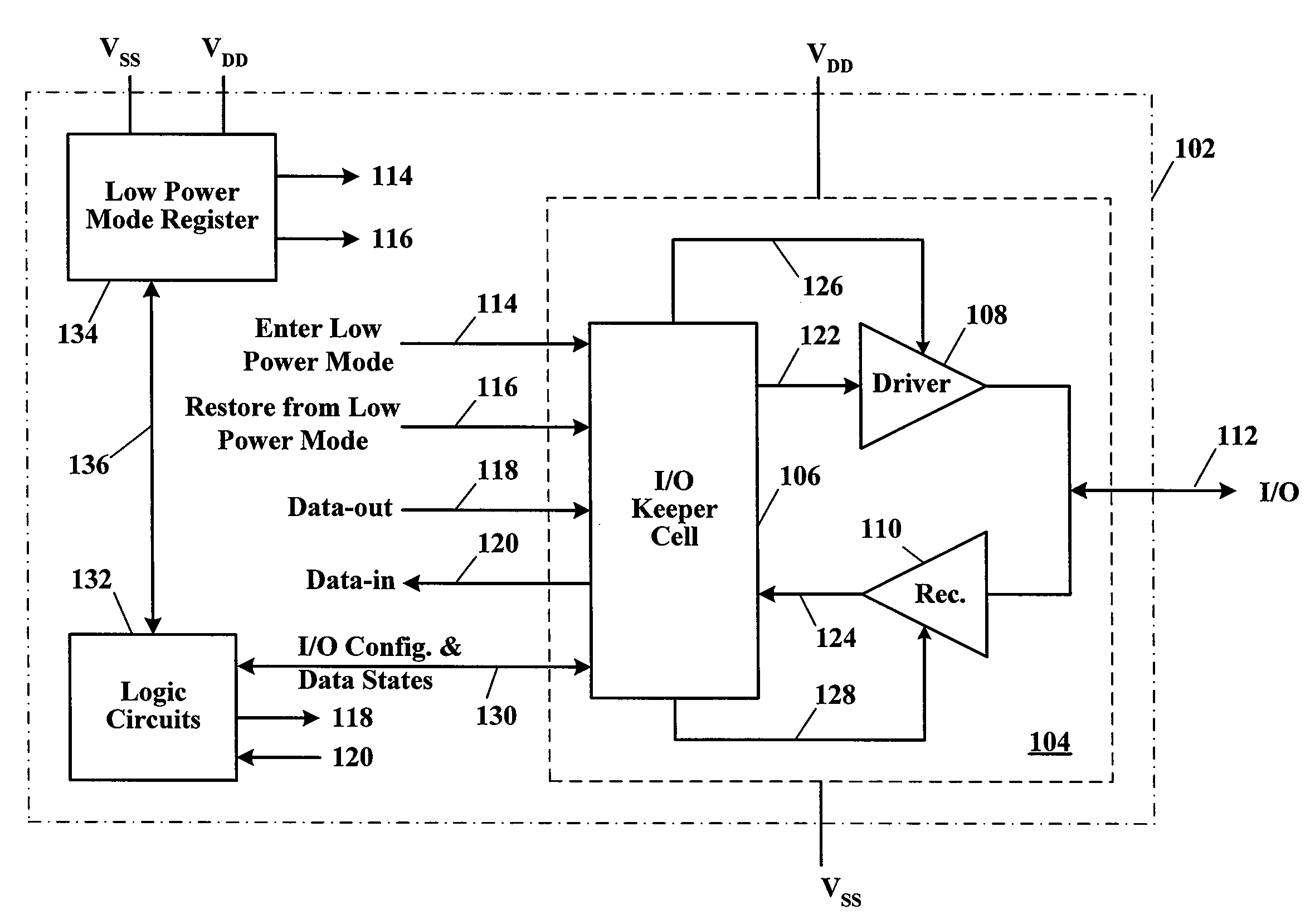
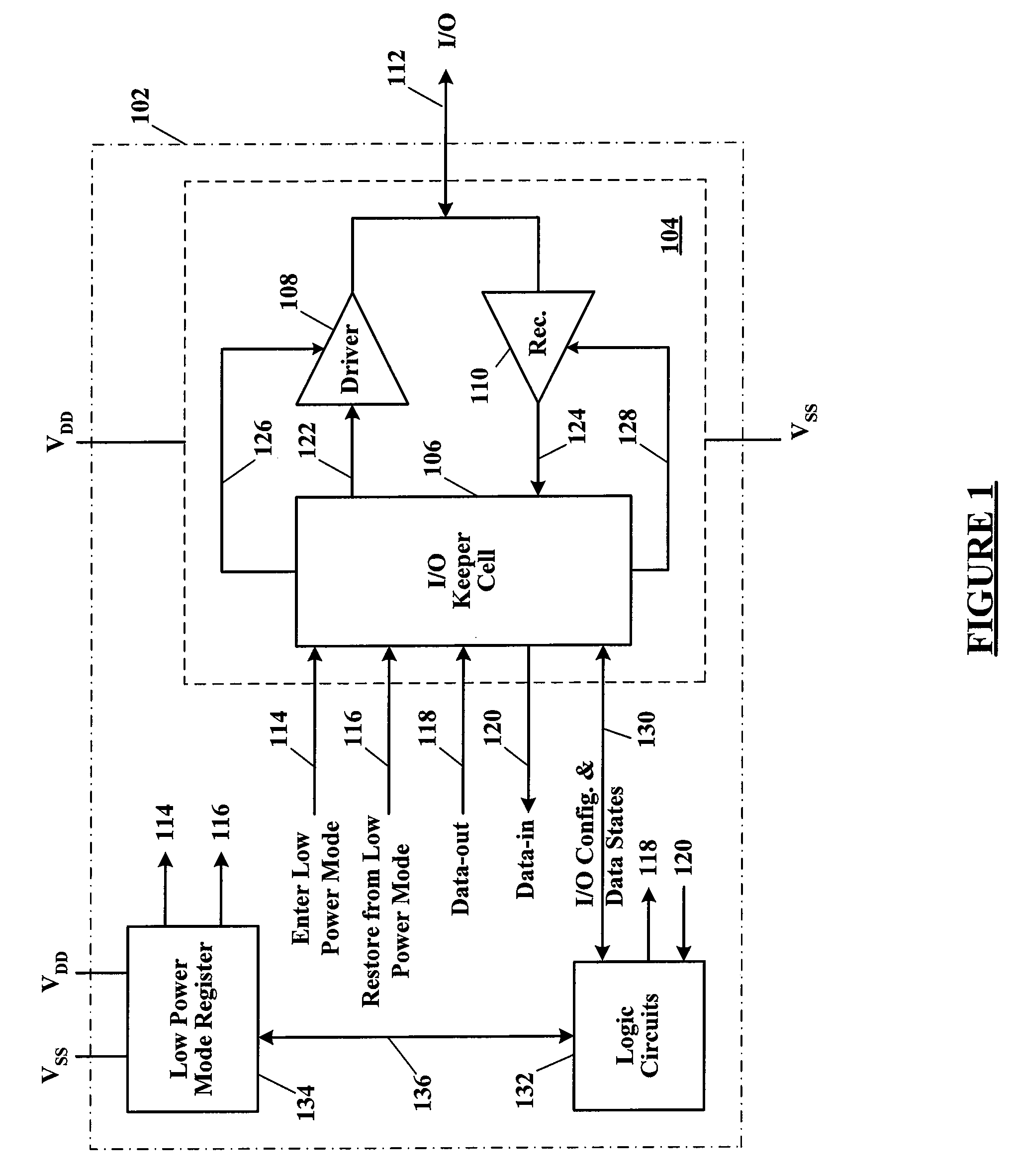
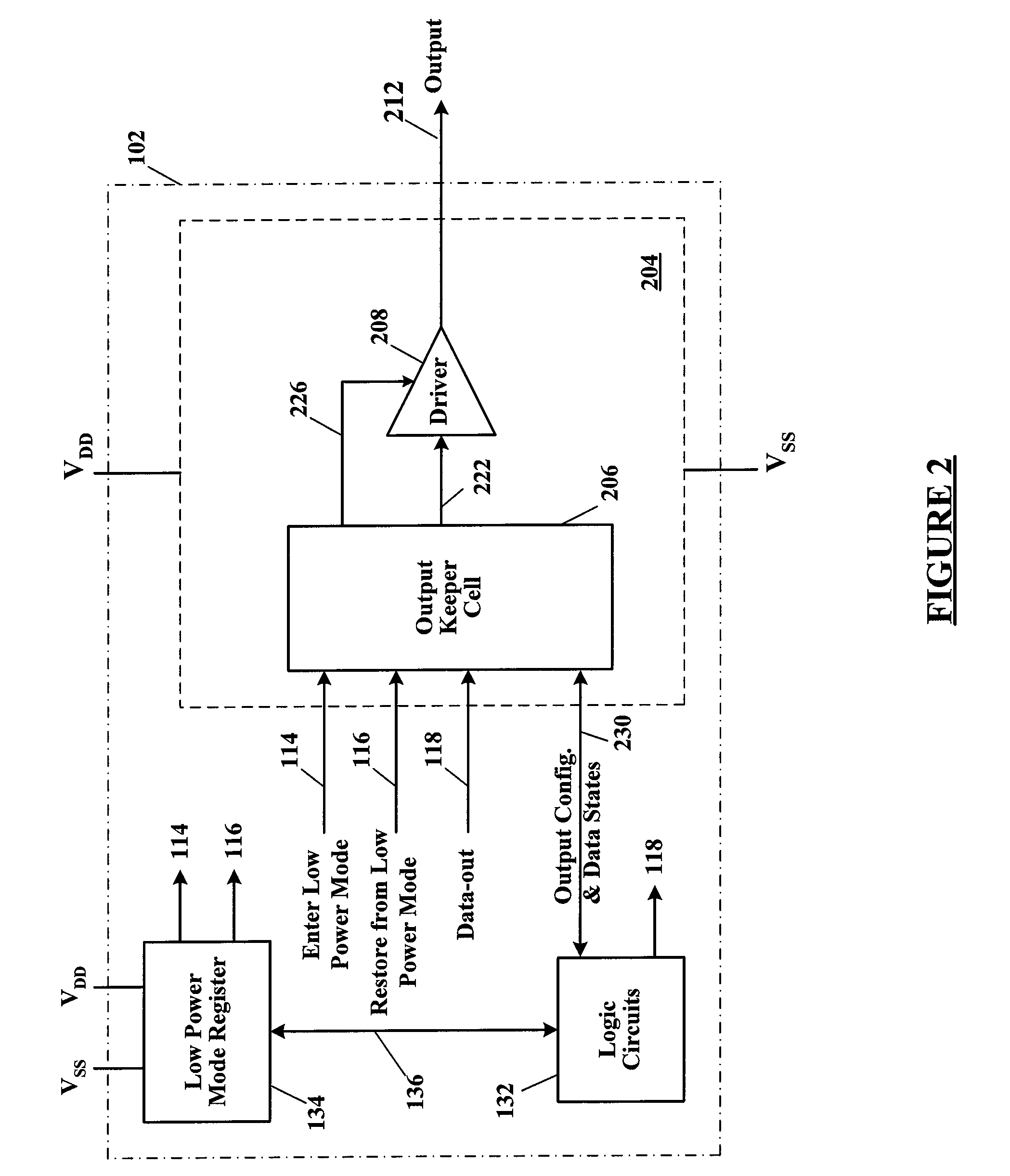
[0018]Referring now to the drawings, the details of specific example embodiments are schematically illustrated. Like elements in the drawings will be represented by like numbers, and similar elements will be represented by like numbers with a different lower case letter suffix.

[0019]Referring to FIG. 1, depicted is a schematic block diagram of an input-output (I / O) node having an I / O keeper cell in an integrated circuit device, according to a specific example embodiment of this disclosure. An integrated circuit device 102, e.g., microprocessor, microcontroller, digital signal processor (DSP), programmable logic array (PLA), application specific integrated circuit (ASIC), etc., may comprise a configurable input-output (I / O) node 104, a low power mode register 134 and a plurality of logic circuits 132, some of which may be coupled to the configurable I / O node 104 and / or the low power mode register 134.

[0020]The configurable I / O node 104 may comprise a driver 108, a receiver 110, and a...


PUM


Abstract

A semiconductor integrated circuit device upon exiting from a low power mode, wakes up and re-initializes logic circuits so as to restore previous logic states of internal registers without disturbing input-output (I / O) configuration control and data states present at the time the low power mode was entered. Thus not distributing the operation of other devices connected to the semiconductor integrated circuit device previously in the low power mode. Once all internal logic and registers of the semiconductor integrated circuit device have been re-initialized, a “low power state wake-up and restore” signal may issue. This signal indicates that the I / O configuration control and data states stored in the I / O keeper cell at the time the integrated circuit device entered into the low power mode have been reinstated and control may be returned to the logic circuits and / or internal registers of the semiconductor integrated circuit device.

Description

TECHNICAL FIELD[0001]The present disclosure relates to a semiconductor integrated circuit device entering into, during and coming out of a low power mode, and more particularly, to maintaining the input and / or output configuration and data state(s) during and when the semiconductor integrated circuit device comes out of the low power mode.BACKGROUND[0002]Integrated circuit devices are being fabricated with decreasing transistor geometry sizes that result in increased leakage currents during operation thereof. One solution to reducing leakage currents when operation of the integrated circuit device is not required is to shut down and / or remove power from some or most of the transistor logic circuits of the integrated circuit device. This puts the transistor logic circuits of the integrated circuit device into a “low power mode” that substantially reduces the power requirements of the integrated circuit device during extended standby conditions.[0003]With current architecture implemen...

Claims


Application Information

Patent Timeline
IPC IPC(8): H03K19/0175
CPCG06F1/3203G06F1/24H03K19/00H03K17/22
Inventor SIMMONS, MICHAELWOJEWODA, IGOR
Owner MICROCHIP TECH INC
Features
  • Generate Ideas
  • Intellectual Property
  • Life Sciences
  • Materials
  • Tech Scout
  • Unparalleled Data Quality
  • Higher Quality Content
  • 60% Fewer Hallucinations
Learn More