Semiconductor device yield prediction system and method

a technology of semiconductor/solid-state device and yield prediction, which is applied in the direction of semiconductor/solid-state device testing/measurement, instruments, computer control, etc., can solve the problems of delayed delivery to customers, most defects generated in the course of manufacturing, and articles going to waste, so as to achieve the effect of predicting yield

Inactive Publication Date: 2008-06-12
HITACHI LTD
View PDF6 Cites 47 Cited by
  • Summary
  • Abstract
  • Description
  • Claims
  • Application Information

AI Technical Summary

Benefits of technology

[0026]According to the present invention, it is possible to predict the yield at the time of receiving an order for a semi-custom IC product, in manufacturing a wide variety of products in small quantities where varieties of electronic devices can be produced by connecting circuit elements (macro-cells) depending on requests of customers. As a result, it is possible to set prices appropriately. Further, since the yield can be predicted accurately in the course of manufacturing, it is possible to control input amounts appropriately.

Problems solved by technology

Most defects generated in the course of manufacturing are generated in the pre-process.
In the case where it is found after the launch of a product that the yield is lower than the predicted value, then delivery to the customer is delayed since no substitute product exists.
On the other hand, in the case where the yield is higher than the predicted value and surplus articles are produced, then those articles go to waste since there is a limited number of customers requiring the product.
A functional failure is a failure as a result of which a circuit does not operate normally, and arises mainly from breaking or shorting of a circuit pattern, which is caused in turn by a dust particle or a pattern defect occurring in the course of manufacturing.
On the other hand, a characteristic failure is a defect as a result of which performance such as operating speed of a transistor or a capacitance of a condenser does not satisfy design specifications, and arises from slight variations in processing: for example, a variation in circuit dimension or oxide film thickness.
However, design layout data of the transistor formation layer have logic gates that are not ultimately connected.
Thus, it is difficult to calculate average fault ratios of all circuit layers in all kinds of gate array products.
However, this method does not consider connection lines between the functional blocks, and it is difficult to forecast an average fault ratio considering effects of all the connection lines.
Thus, it is difficult to calculate respective average fault ratios of the random logic parts.
Thus, although it is considered that the yield prediction of the conventional method is sufficiently accurate for pricing a product at the time of receiving an order for the product, the accuracy of the conventional prediction method is low for controlling input.

Method used


Image

  • Semiconductor device yield prediction system and method
  • Semiconductor device yield prediction system and method
  • Semiconductor device yield prediction system and method

Examples


example 1

[0068]A yield prediction system of one embodiment of the present invention will now be described referring to the drawings.

[0069]The yield prediction system of the present embodiment predicts a yield that results from functional failures with respect to an electronic device product B (a prediction target product) at the time when an order for the product is received.

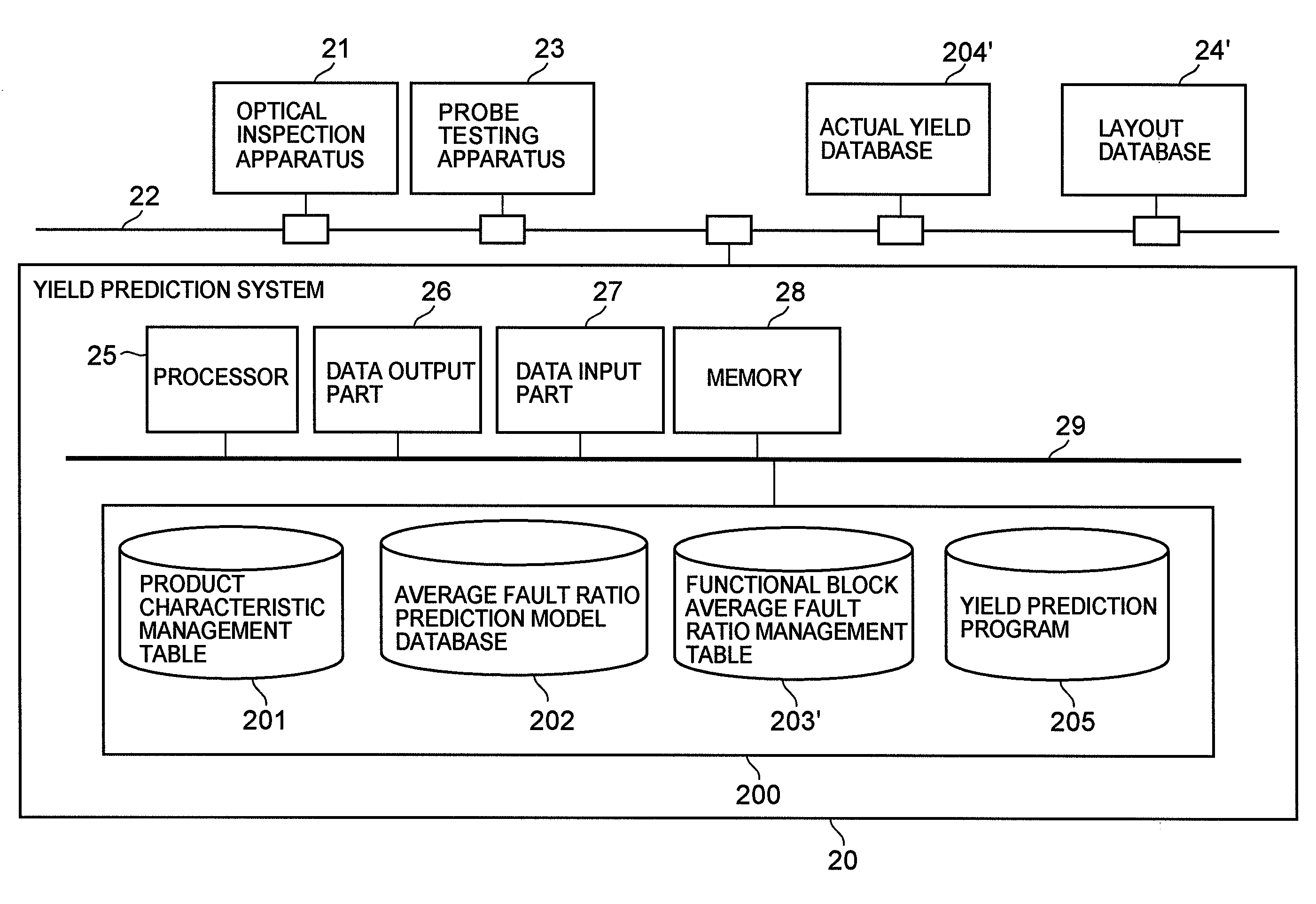
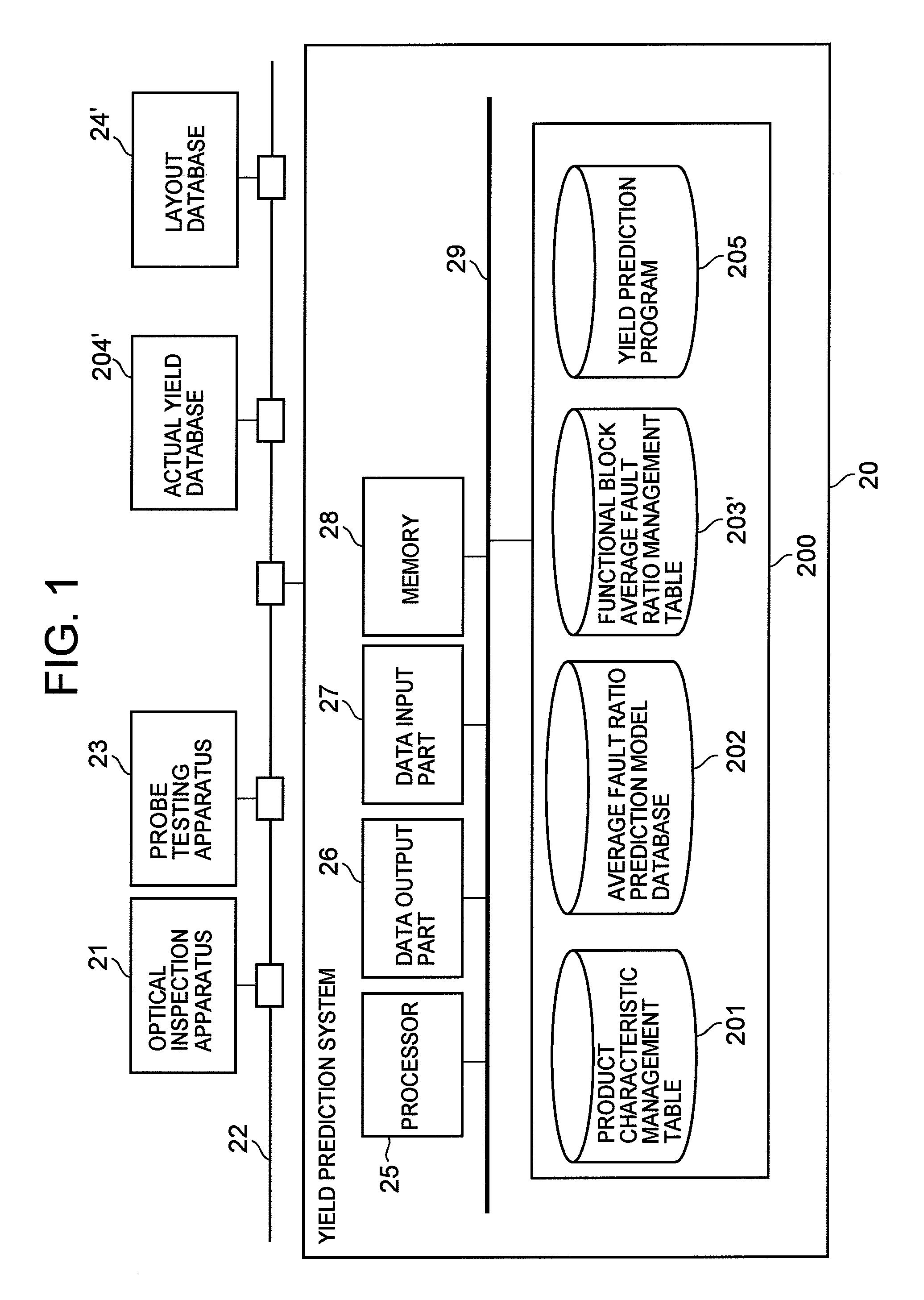
[0070]A configuration of the yield prediction system of the present embodiment will be described. FIG. 1 is a block diagram showing a configuration of the yield prediction system of the present embodiment. As shown in the figure, the yield prediction system 20 of the present embodiment is connected to external units, namely, a optical inspection apparatus 21, an probe testing apparatus 23, an actual yield database 204′ and a layout database 24′ through a local area network 22.

[0071]The optical inspection apparatus 21 is an inline inspection apparatus that detects defects such as dust particles and pattern defects optical...

example 2

[0108]Next, another yield prediction system of one embodiment of the present invention will be described referring to drawings.

[0109]The yield prediction system of the present embodiment predicts a yield that results from functional failures, in the course of manufacturing an electronic device product B (a prediction target product).

[0110]In the present embodiment, optical inspection and electrical inspection are performed on another product A (a reference product) that has already been produced on the manufacturing line, and these inspection results are used for prediction of a yield of the product B. Here, it is assumed that the product A and the product B are family products manufactured in similar processes. In detail, it is assumed that the product A and the product B have the same stacked layer structure although their circuit patters are different, each having structure of staking of one or more circuit layers a, b, c, . . . in order. Further, it is also assumed that the prod...


PUM


Abstract

An average fault ratio is calculated from product characteristics of a product as a target of yield prediction, in order to predict yield accurately in the course of manufacturing the prediction target product.
With respect to a reference product, whose wiring pattern is different from the prediction target product but manufactured by the same manufacturing process, a monthly electric fault density is calculated from actually measured data. Respective average fault ratios are obtained from product characteristics of the prediction target product and the reference product. A monthly electric fault density of the prediction target product is obtained by multiplying the monthly electric fault density of the reference product by the ratio of the average fault ratios. The yield is calculated by using the monthly electric fault density of the month in which a yield prediction target lot of the prediction target product was processed.

Description

BACKGROUND OF THE INVENTION[0001]The present invention relates to a technique of predicting yields of an electronic device such as a semiconductor integrated circuit at the time when an order for the product is received and at the time when the product is manufactured, and particularly to a technique of predicting yields of a semi-custom IC from which kinds of electronic devices can be produced by connecting circuit elements (macro-cells) depending on requests of customers.[0002]Generally, a manufacturing process of an electronic device represented by a semiconductor integrated circuit can be broadly divided into a pre-process in which a plurality of chips are produced by stacking layers, such as circuit pattern layers, on a silicon wafer, and a post-process in which the silicon wafer is cut into individual chips to complete a product. Most defects generated in the course of manufacturing are generated in the pre-process. Accordingly, improvement in yield in the pre-process holds th...

Claims


Application Information

Patent Timeline
Patent Type & Authority Applications(United States)
IPC IPC(8): G06F17/18G06F19/00H01L21/66
CPCG05B17/02G05B15/02
Inventor MORIOKA, NATSUYOISHIKAWA, SEIJIIKEGAYA, KATSUMIYAMAGUCHI, YASUNORIITO, KAZUOHAMAMURA, YUICHI
Owner HITACHI LTD
Why Eureka
Try Eureka