Method of manufacturing multilayer electronic component

a technology of electronic components and manufacturing methods, applied in the direction of fixed capacitors, stacked capacitors, fixed capacitor details, etc., can solve the problems of reducing reliability, difficult step of applying conductive paste to specific portions, and low density and homogeneity of formed plating films, so as to improve the effective volume ratio

Inactive Publication Date: 2008-06-19
MURATA MFG CO LTD
View PDF23 Cites 32 Cited by
  • Summary
  • Abstract
  • Description
  • Claims
  • Application Information

AI Technical Summary

Benefits of technology

[0014]To overcome the problems described above, preferred embodiments of the present invention provide a method of manufacturing a multilayer electronic component having an improved effective volume ratio in which an external electrode is substantially formed using only a plating deposit.
[0015]Preferred embodiments of the present invention also provide a method of manufacturing a multilayer electronic component capable of simply forming an external electrode composed of a dense plating film without complicated previous steps, e.g., a step of coating conductive paste and a step of applying a catalyst, and capable of ensuring high reliability.
[0030]According to preferred embodiments of the present invention, it is possible to simply form at least a portion of an external electrode which is directly connected to the internal electrodes using a dense electroless plating deposit having high homogeneity without complicated previous steps, e.g., a step of coating conductive paste and a step of applying a catalyst. As a result, a multilayer electronic component which maintains high reliability is obtained.
[0031]Further, according to preferred embodiments of the present invention, an electroless plating film having a high density is obtained without using a metal having high catalytic activity, such as Pd or Pt, as the main component of the internal electrodes. Therefore, an inexpensive metal material, such as Ni, Cu, or Ag, can be used for the internal electrodes, and thus, a multilayer electronic component can be obtained at a reduced cost.
[0032]Further, even when the thickness of the internal electrodes is less than about 1 μm, a dense electroless plating film is formed, and thus, a small multilayer electronic component is obtained at a reduced cost.
[0033]When the average diameter of the conductive medium is at least about 0.2 mm, the formation efficiency of a plating film is further improved.

Problems solved by technology

The step of applying the conductive paste to specific portions is difficult.
On the other hand, the electroless plating method described in Japanese Unexamined Patent Application Publication No. 63-169014 has a problem in that the formed plating films have low density and homogeneity, and a plating solution easily penetrates into the laminate to decrease reliability.
However, there is a problem in that the step of applying a catalyst is complicated, and the plating films are easily deposited in portions other than desired portions.
Thus, there is a problem of a low degree of freedom of the selection of a metal material to be used for the internal electrodes.
In addition, since Pd and Pt are expensive noble metals, there is a problem of increasing the cost of a multilayer electronic component.
Furthermore, in the method described in Japanese Unexamined Patent Application Publication No. 63-169014, the thickness of the internal electrodes must be at least about 1 μm, and thus, there is a problem of increasing the size of a laminate and increasing the cost of a multilayer electronic component.

Method used


Image

  • Method of manufacturing multilayer electronic component
  • Method of manufacturing multilayer electronic component
  • Method of manufacturing multilayer electronic component

Examples


experimental example 1

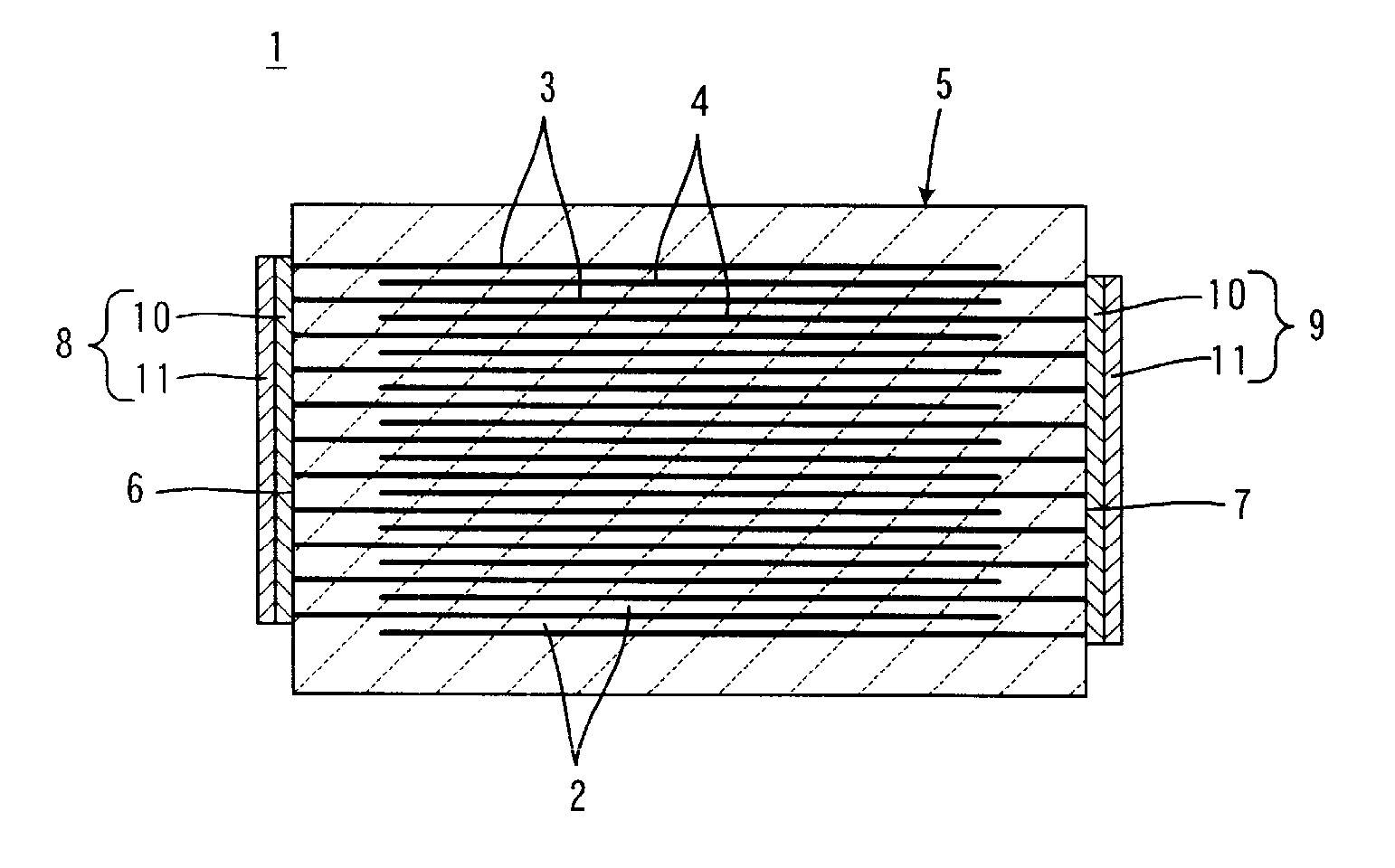
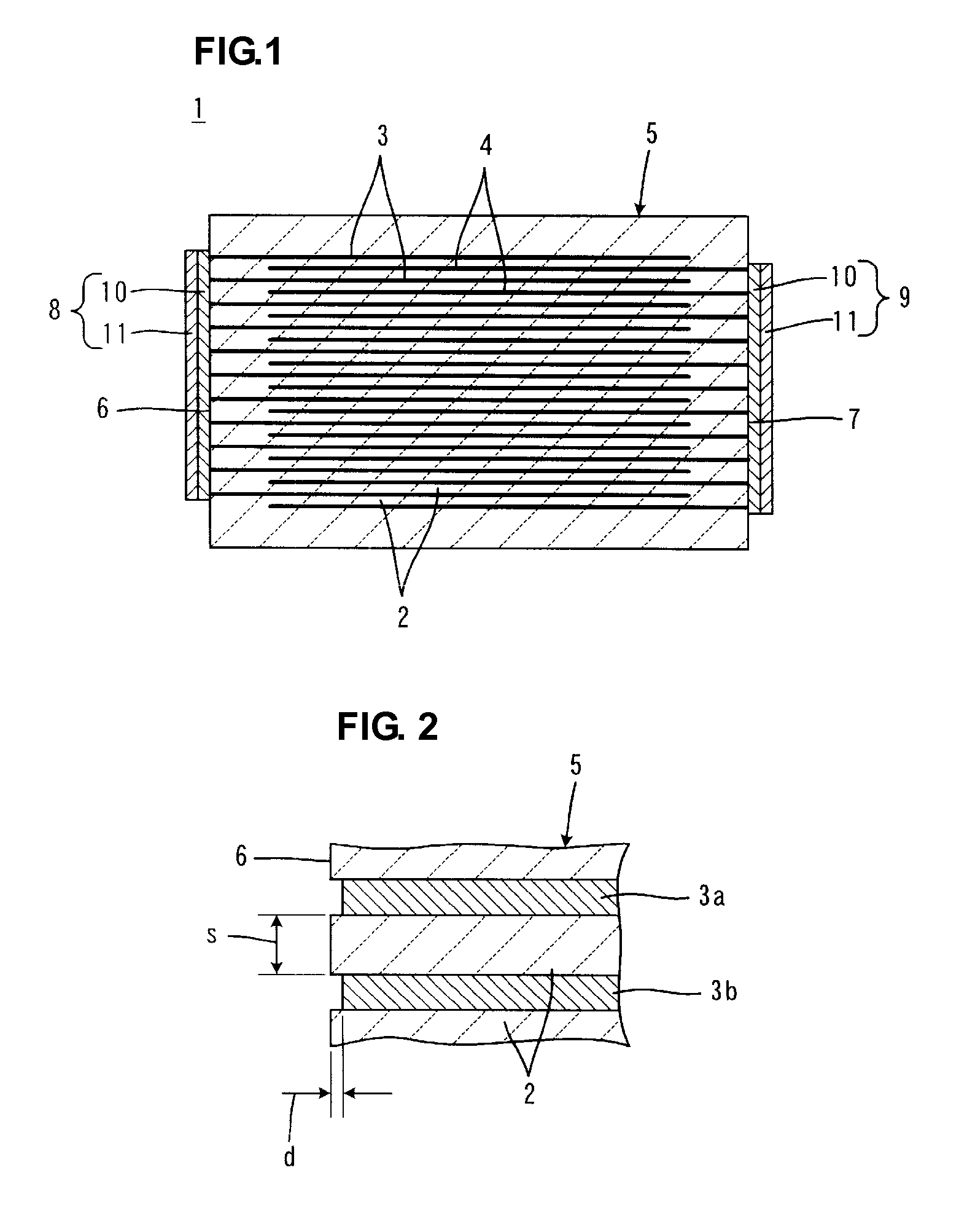
[0107]In Experimental Example 1, conductive media made of different materials were prepared for use in electroless plating. In a multilayer electronic component shown in FIG. 1, the influences of the materials used for the conductive media were examined when a first plating layer was formed, by electroless plating, directly on each of the end surfaces of a laminate in which internal electrodes were exposed.

[0108]In detail, a multilayer ceramic capacitor laminate having a length of about 1.6 mm, a width of about 0.8 mm, and a thickness of about 0.8 mm was prepared as a material to be plated, and the laminate included insulator layers composed of a barium titanate-based dielectric material and internal electrodes, the thickness and the main component of the internal electrodes being as shown in “Thickness of internal electrode” and “Main component of internal electrode” in Table 2. In the laminate, the thickness of the insulator layers, i.e., the distance “s” between the adjacent inte...

experimental example 2

[0116]In Experimental Example 2, the influence of the thickness of internal electrodes in a laminate on the quality of electroless plating was examined.

[0117]The same laminate as in Experimental Example 1 was used as a material to be plated except that the thickness and the main component of the internal electrodes were as shown in “Thickness of internal electrode” and “Main component of internal electrode” in Table 3.

[0118]Next, 5000 of the laminates and about 50 cc of each conductive medium having a diameter of about 0.2 mm were placed in a rotary barrel having a volume of about 300 cc, and an electroless Ni plating film having a thickness of about 8 μm was formed as a first plating layer on each of the end surfaces of each laminate, at which the internal electrodes were exposed, under the conditions A shown in Table 1 as shown in “Plating condition” in Table 3. In this case, the material of the conductive medium used was either Fe or Ni as shown in the column “Type of conductive ...

experimental example 3

[0125]In Experimental Example 3, the influence of barreling before electroless plating was examined, and first plating layers were formed by electroless plating using various metal ions or reducing agents.

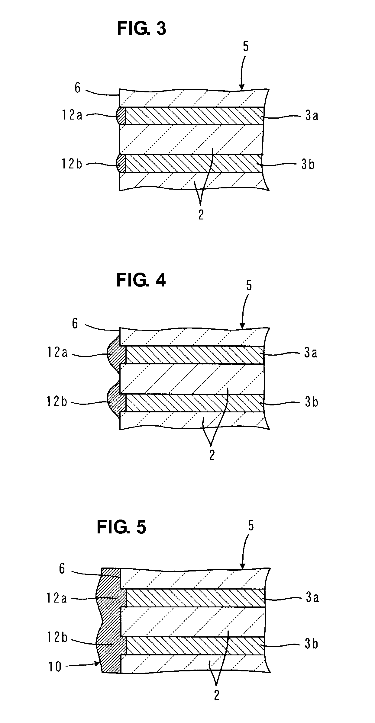
[0126]The same laminate as in Experimental Example 1 was used as a material to be plated except that the thickness and the main component of the internal electrodes were as shown in “Thickness of internal electrode” and “Main component of internal electrode” in Table 4. Therefore, the withdrawn length “d” of the internal electrodes from each of the end surfaces of the laminate, in which the internal electrodes were exposed, was about 2.0 μm which was the same as in Experimental Example 1.

[0127]Next, as shown in Table 4, the laminate of each of Samples 22, 23, 24, 25, 26, 28, and 30 was barreled with an abrasive agent so that the maximum withdrawn length “d” of the internal electrodes from each of the end surfaces of the laminate, in which the internal electrodes were exposed, was a...


PUM

PropertyMeasurementUnit
diameteraaaaaaaaaa
lengthaaaaaaaaaa
lengthaaaaaaaaaa

Abstract

An electroless plating step for forming external electrodes includes preparing a plating solution including a reducing agent and metal ions having a more electochemically positive deposition potential than the oxidation-reduction potential of the reducing agent, placing a laminate for a multilayer electronic component together with a conductive medium having catalytic activity for an oxidation reaction of the reducing agent in a vessel, and stirring the laminate and the conductive medium in the plating solution by rotation, shaking, inclination, or vibration. Electroless plating proceeds to connect each other plating deposits deposited on the ends of a plurality of internal electrodes.

Description

BACKGROUND OF THE INVENTION[0001]1. Field of the Invention[0002]The present invention relates to a method of manufacturing a multilayer electronic component, and particularly to a method of manufacturing a multilayer electronic component in which external electrodes are formed directly on the outer surfaces of a laminate by electroless plating.[0003]2. Description of the Related Art[0004]As shown in FIG. 11, a multilayer electronic component 101 represented by a multilayer ceramic capacitor includes a laminate 105 including a plurality of stacked insulator layers 102 and a plurality of internal electrodes 103 and 104 arranged along the interfaces between the respective insulator layers. The ends of the plurality of internal electrodes 103 and 104 are exposed at the ends 106 and 107, respectively, of the laminate 105, and external electrodes 108 and 109 are arranged to electrically connect the ends of the internal electrodes 103 and 104, respectively.[0005]To form the external electr...

Claims


Application Information

Patent Timeline
Patent Type & Authority Applications(United States)
IPC IPC(8): B05D1/18B05D5/12
CPCH01G4/12H01G4/2325H01G4/30H01G13/006
Inventor KUNISHI, TATSUOOGAWA, MAKOTOMOTOKI, AKIHIRO
Owner MURATA MFG CO LTD
Why Eureka
Try Eureka