Insulated gate bipolar transistor with enhanced conductivity modulation

a bipolar transistor and conductivity modulation technology, applied in the field of electronic devices, can solve the problems of limiting the number of igbt cells that can be fabricated on a single wafer, poor on-state loss, and high drift resistance, and achieves improved conductivity modulation, reduced on-state power dissipation, and enhanced modulation layer

Inactive Publication Date: 2008-07-03
NORTHROP GRUMMAN SYST CORP
View PDF7 Cites 24 Cited by
  • Summary
  • Abstract
  • Description
  • Claims
  • Application Information

AI Technical Summary

Benefits of technology

[0006]A insulated gate bipolar transistors (IGBT) having an enhanced modulation layer provides reduced on-state power dissipation and better conductivity modulation than conventional devices. The IGBT includes an enhanced modulation layer disposed within a portion of the n− doped drift layer, in a n-type device, or p− doped drift layer, in a p-type device. The enhanced modulation layer contains a higher carrier concentration than the n− or p− doped drift layer. If the IGBT de...

Problems solved by technology

Although using thick, lightly doped semiconductor layers allows the device to handle high blocking voltages, this configuration also leads to high drift resistance and poor on-state losses.
However, conve...

Method used


Image

  • Insulated gate bipolar transistor with enhanced conductivity modulation
  • Insulated gate bipolar transistor with enhanced conductivity modulation
  • Insulated gate bipolar transistor with enhanced conductivity modulation

Examples


Embodiment Construction

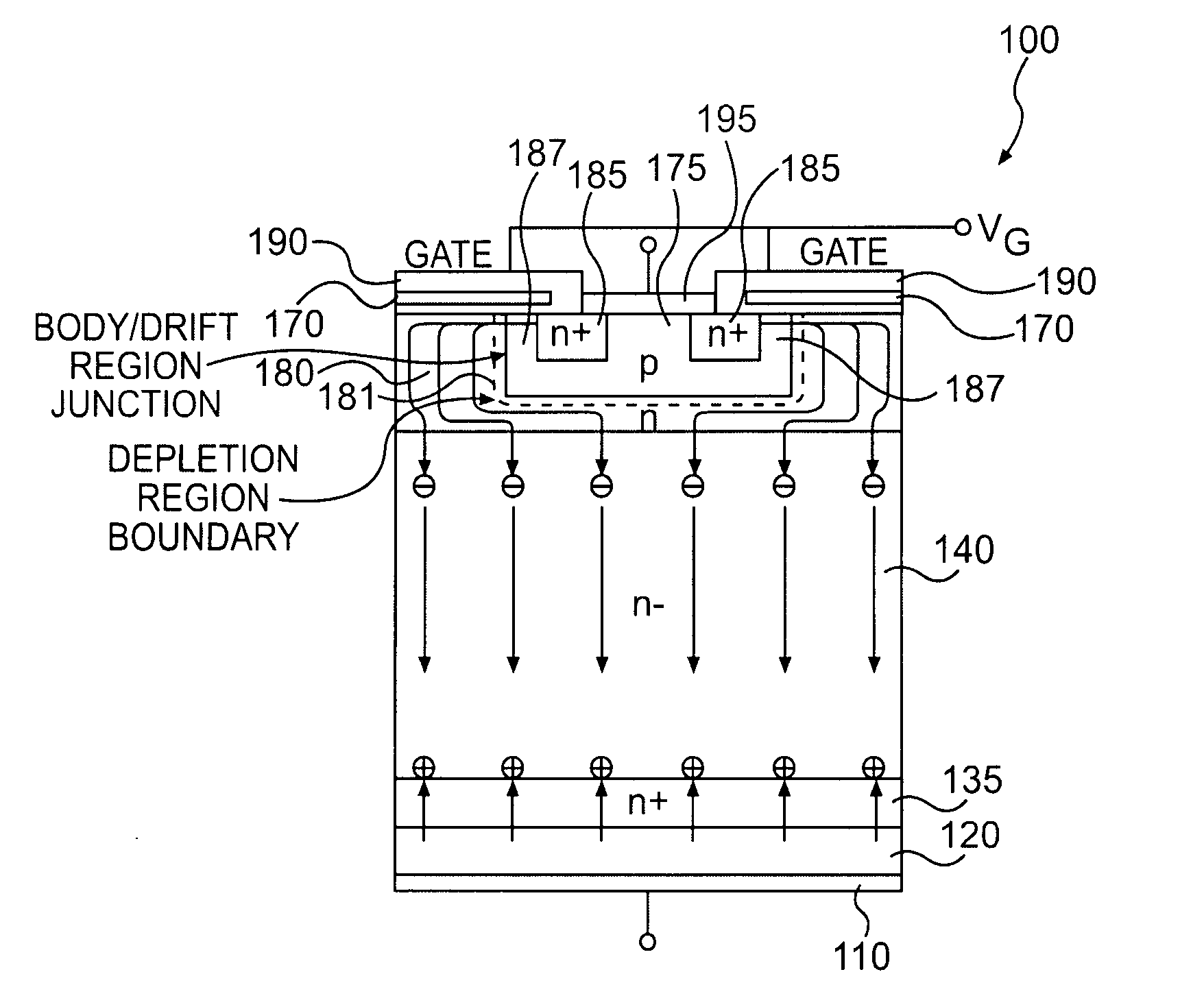
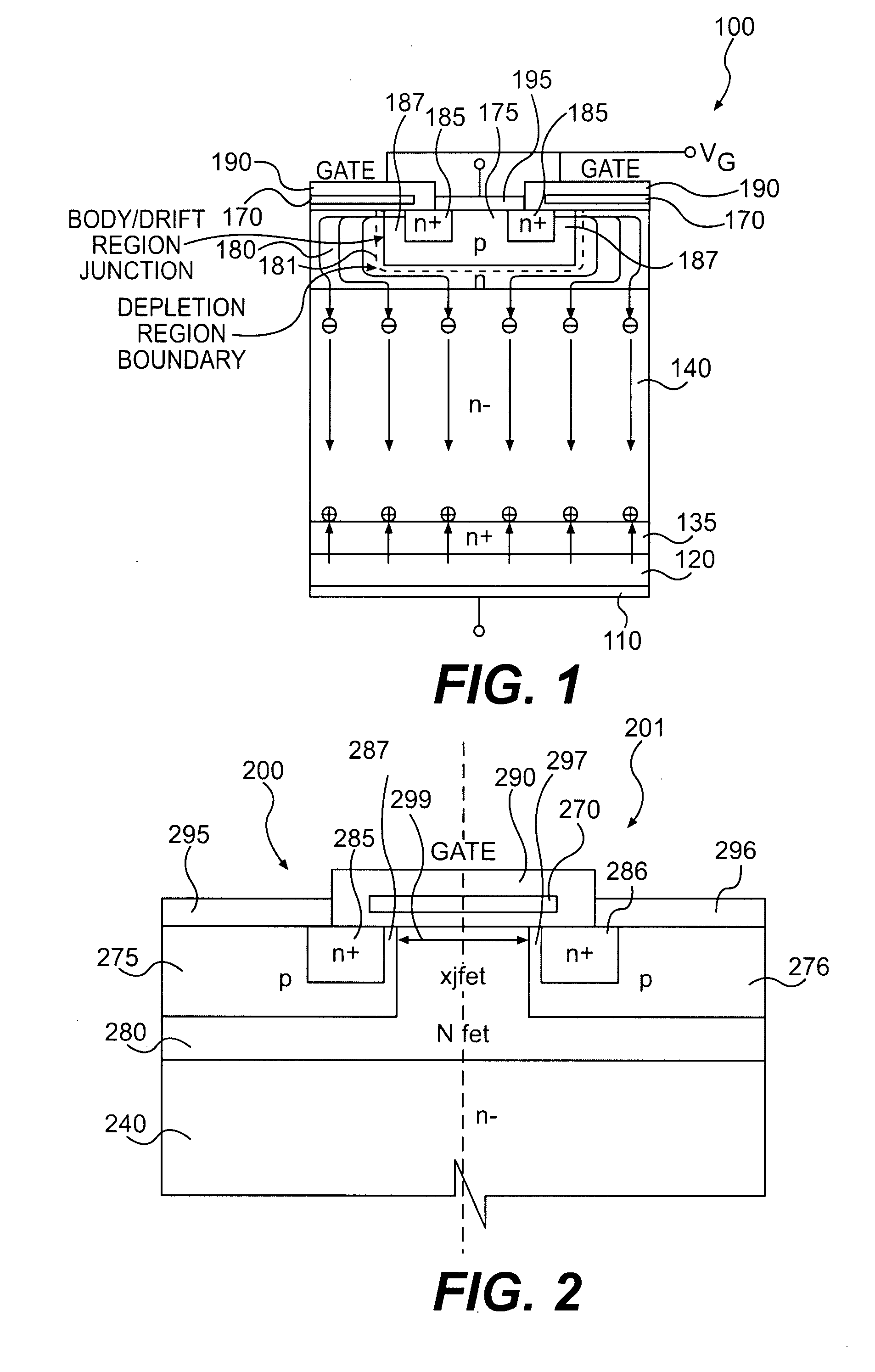
[0012]FIG. 1 illustrates a single cell of a n-type insulated gate bipolar transistor (IGBT) cell 100 incorporating an enhanced modulation layer. An IGBT device may include a plurality of IGBT cells fabricated on a single silicon carbide (SiC) wafer, for example. Other materials, such as silicon, gallium nitride (GaN), gallium arsenide (GaAs) may be used for device fabrication.

[0013]The IGBT cell 100 includes a emitter 110, a collector 195, and a gate 170. The collector 195 and emitter 110 may be metal electrodes, and the gate 170 may be a poly-silicon gate. The emitter 110 is coupled to p+ doped injecting layer 120. A n− doped drift layer 140 is disposed on the p+ doped injecting layer 120. A p well body region 175 is disposed on the n− doped drift layer 140. The n− doped drift layer 140 is located between the p+ doped injecting layer 120 and the p well body region 175. As shown, n+ regions 185 are disposed in the p well body region 175. A channel 187 is formed in the surface of the...


PUM


Abstract

A insulated gate bipolar transistors (IGBT) having an enhanced modulation layer provides reduced on-state power dissipation and better conductivity modulation than conventional devices. The IGBT includes an enhanced modulation layer disposed within a portion of the n− doped drift layer, in a n-type device, or p− doped drift layer, in a p-type device. The enhanced modulation layer contains a higher carrier concentration than the n− or p− doped drift layer. If the IGBT device is in an on state, the enhanced modulation layer decreases a size of a depletion region formed around the p well body region or n well body region. In a n-type enhanced modulation layer IGBT, electrons, traveling from the n+ region towards the emitter, are spread laterally and uniformly in the n− doped drift layer. In a p-type enhanced modulation layer IGBT, holes, traveling from the p+ region towards the emitter, are spread laterally and uniformly in the p− doped drift layer.

Description

[0001]The invention was made under a contract with an agency of the United States Government, contract number N00014-05-C-0203.FIELD OF THE INVENTION[0002]The invention relates generally to electronic devices, specifically to an insulated gate bipolar transistor with enhanced conductivity modulation and methods of making same.BACKGROUND OF THE INVENTION[0003]Metal oxide field effect transistors (MOSFETs) and insulated gate bipolar transistors (IGBT) are typically manufactured using silicon. The MOSFET is often used for lower voltages (e.g., <600 V) while an IGBT can be used for voltages between, for example, 600 V and 6.5 kV. One of the reasons for using an IGBT over a MOSFET device is the trade-off between on-state losses and switching losses. The n-channel MOSFET is a uni-polar device, generally relying on electrons to carry the current. When designing a MOSFET to handle high blocking voltages (off state blocking), thick, lightly doped semiconductor layers are used. Although us...

Claims


Application Information

Patent Timeline
IPC IPC(8): H01L29/74H01L21/332
CPCH01L29/0692H01L29/1095H01L29/7395
Inventor MCNUTT, TY R.WALDEN, GINGER G.SHERWIN, MARC E.
Owner NORTHROP GRUMMAN SYST CORP
Why Eureka
Try Eureka