MTCMOS Flip-Flop Circuit

a flip-flop circuit and flip-flop technology, applied in the field of mtcmos flip-flop circuits, can solve the problems of circuit malfunction, large size of a transistor used as a switch, complicated design flow, etc., and achieve the effect of minimizing the leakage curren

Inactive Publication Date: 2008-07-03
DONGBU HITEK CO LTD
View PDF4 Cites 10 Cited by
  • Summary
  • Abstract
  • Description
  • Claims
  • Application Information

AI Technical Summary

Benefits of technology

[0007]Accordingly, embodiments of the present invention provide an MTCOMS flip-flop circuit capable of retaining data (latched signals) in a sleep mode, implementing high-speed and low-power consumption in an active mode, and minimizing a leakage current in a sleep mode.

Problems solved by technology

In addition, since the size of a MOS transistor used for serial connection should be large to properly transmit data to the latch, the size of a transistor used as a switch may become large.
This may be a burden when routing an actual circuit.
For this reason, a complicated design flow is necessary to prevent malfunction of the circuit.
This results in increasing TAT (Turn Around Time) for a design and increasing design costs.
However, if the size of the MOS transistor is reduced to prevent such a leakage current, the speed of the circuit may be decreased during normal operation.

Method used


Image

  • MTCMOS Flip-Flop Circuit
  • MTCMOS Flip-Flop Circuit
  • MTCMOS Flip-Flop Circuit

Examples


first embodiment

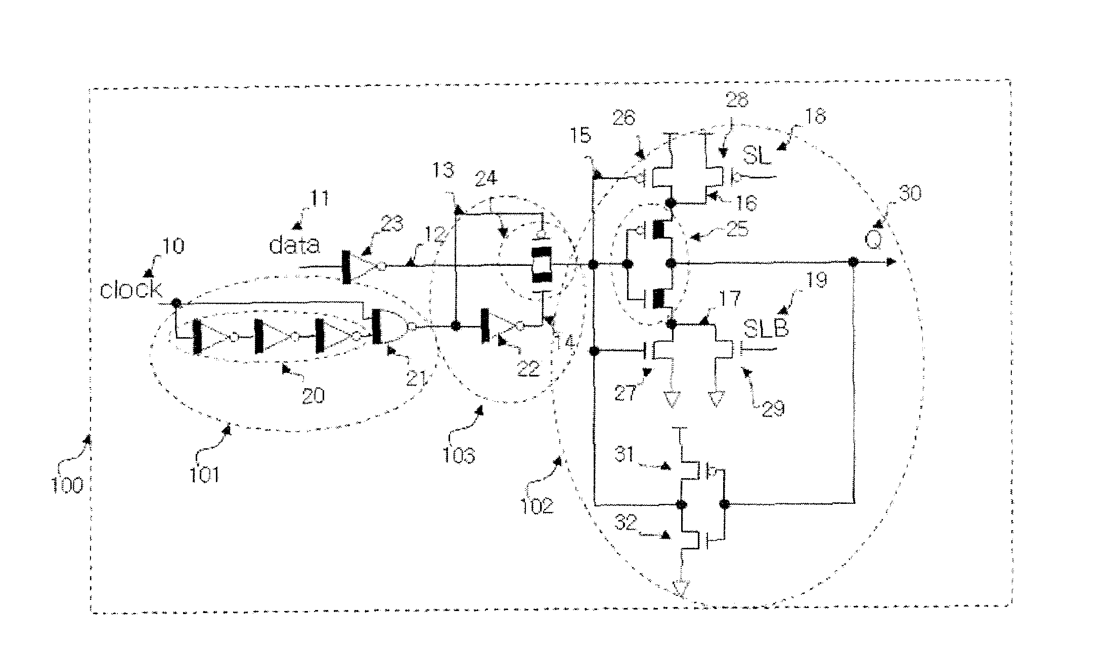
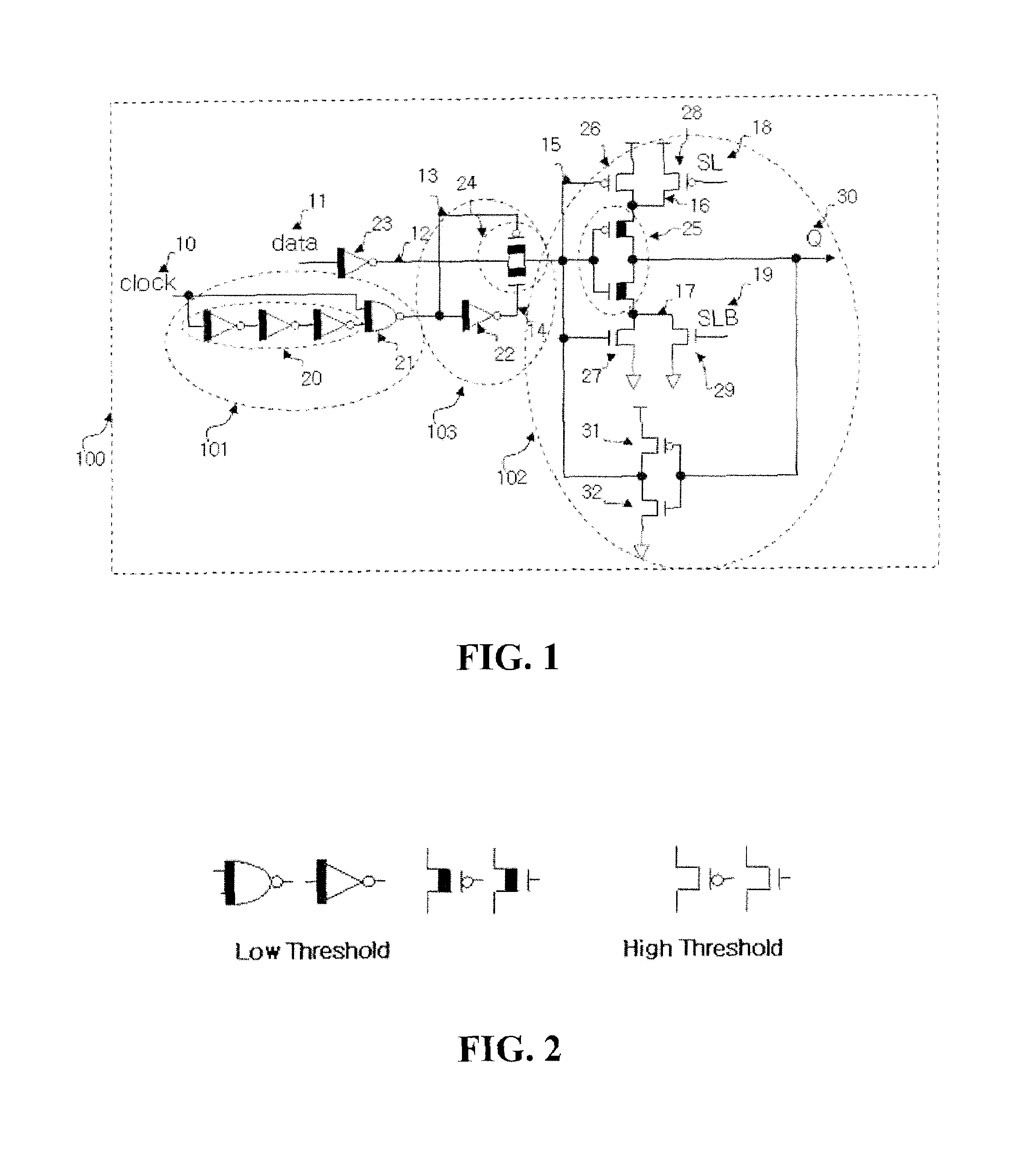
[0020]FIG. 1 is a circuit diagram of an MTCMOS flip-flop circuit according to a

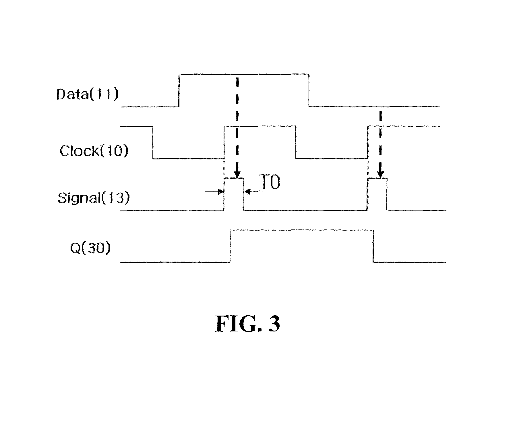
[0021]As illustrated in FIG. 1, the MTCMOS flip-flop circuit 100 includes a clock signal generator 101 for generating clock control signals 13 and 14 for latching a data signal 11 at a rising time of a clock signal using an input clock 10.

[0022]The MTCMOS flip-flop circuit 100 can further include a data transmitting unit 103 for transmitting the input data signal 11 to a post stage, and a data latch and output unit 102 for storing a signal output from the data transmitting unit 103.

[0023]In the MTCMOS flip-flop circuit 100 according to the first embodiment, a pulsed clock is generated, an output is not floated in a sleep mode, and a high-speed operation is possible.

[0024]In a specific embodiment of the MTCMOS flip-flop circuit 100, a data input unit 23 includes an inverter for receiving an input data signal 11, inverting the input data signal 11, and outputting the inverted data signal to be an input of a...

second embodiment

[0048]FIG. 5 is a circuit diagram of an MTCMOS flip-flop circuit according to a

[0049]In the MTCMOS flip-flop circuit according to the second embodiment, the NAND gate 21 for generating a pulsed clock in the MTMOS flip-flop circuit according the first embodiment is replaced with an Exclusive-OR gate 61.

[0050]FIG. 6 is a signal diagram of the MTCMOS flip-flop circuit according to the second embodiment.

[0051]According to the second embodiment, whenever an input clock signal 10 is toggled, a pulsed clock is generated. FIG. 5 illustrates such a circuit.

[0052]As illustrated in FIGS. 5 and 6, a pulsed clock 63 having a pulse width T1 and a pulsed clock 64 that is an inverted signal of the pulsed clock 63 allow a transmission gate including an NMOS transistor and a PMOS transistor (switch 24) to be turned on such that a data 11 is transmitted to a latch unit that is a post stage.

[0053]Accordingly, since the circuit of FIG. 5 can process a double amount of data at the same clock frequency, t...


PUM


Abstract

Disclosed is a multi-threshold CMOS (MTCMOS) flip-flop circuit. The MTCMOS flip-flop circuit includes a data input unit including an inverter for receiving an input data signal, inverting the input data signal and then outputting an inverted data signal; a clock signal generator including an inverter for receiving an input clock signal and a logic gate for generating a pulsed clock for latching the inverted data signal at a rising time of the input clock signal; a data transmitting unit including a switch for receiving the data signal output from the data input unit to selectively output the inverted data signal and controlling transmission of data based on the pulsed clock; and a data latch and output unit including a feedback inverter having a feedback path used for data latch so as to receive the inverted data signal and generate an output Q.

Description

CROSS-REFERENCE TO RELATED APPLICATION[0001]The present application claims the benefit under 35 U.S.C. §119 of Korean Patent Application No. 10-2006-0136394, filed Dec. 28, 2006, which is hereby incorporated by reference in its entirety.BACKGROUND[0002]In the implementation of a multi-threshold CMOS (hereinafter, referred to as a MTCMOS), a high-speed low-power flip-flop circuit can be used to retain data in a sleep mode.[0003]In a conventional MTCMOS flip-flop circuit, since switches used for data transmission in a data transmitting unit are connected in series, the speed of data being transmitted to a latch may be reduced. In addition, since the size of a MOS transistor used for serial connection should be large to properly transmit data to the latch, the size of a transistor used as a switch may become large.[0004]In the conventional MTCMOS flip-flop circuit, an inverter at an output terminal is connected to a virtual power line of an MTCMOS, and thus an output signal is floated ...

Claims


Application Information

Patent Timeline
Patent Type & Authority Applications(United States)
IPC IPC(8): H03K3/356
CPCH03K3/356156H03K3/356121G11C7/10G11C7/22
Inventor KIM, MIN HWAHN
Owner DONGBU HITEK CO LTD
Why Eureka
Try Eureka