Method and apparatus for creating time-resolved emission images of integrated circuits using a single-point single-photon detector and a scanning system

a scanning system and integrated circuit technology, applied in the field of imaging technology, can solve the problems of high time jitter, complicated manufacturing of even single-pixel photodetectors with low noise and low jitter, and prevent their adoption for pica measurements, etc., to achieve the effect of simplifying the interpretation of data

Inactive Publication Date: 2008-07-10
IBM CORP
View PDF9 Cites 29 Cited by
  • Summary
  • Abstract
  • Description
  • Claims
  • Application Information

AI Technical Summary

Benefits of technology

[0008]The evolution and improvement of PICA capabilities may be influenced by different photodetectors adapted to measure the arrival time of the photons compared to a reference signal (trigger). Some detectors like the MEPSICRON S-25™ photo-multiplier tube (PMT) may be employed beca...

Problems solved by technology

Although promising, all prototypes of new imaging photodetectors so far developed have significant disadvantages (such as high noise, hot-spots, non-uniformity, high time jitter) that precluded their adoption for PICA measurements.
In fact, manufacturing even single pixel photodetectors with low noise and low jitter is complicated and leads to a very low yield, and high cost.
The manufacturing technology d...

Method used


Image

  • Method and apparatus for creating time-resolved emission images of integrated circuits using a single-point single-photon detector and a scanning system
  • Method and apparatus for creating time-resolved emission images of integrated circuits using a single-point single-photon detector and a scanning system
  • Method and apparatus for creating time-resolved emission images of integrated circuits using a single-point single-photon detector and a scanning system

Examples


Embodiment Construction

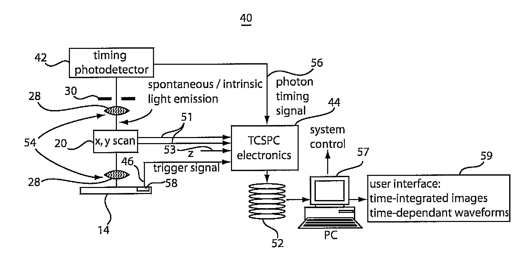
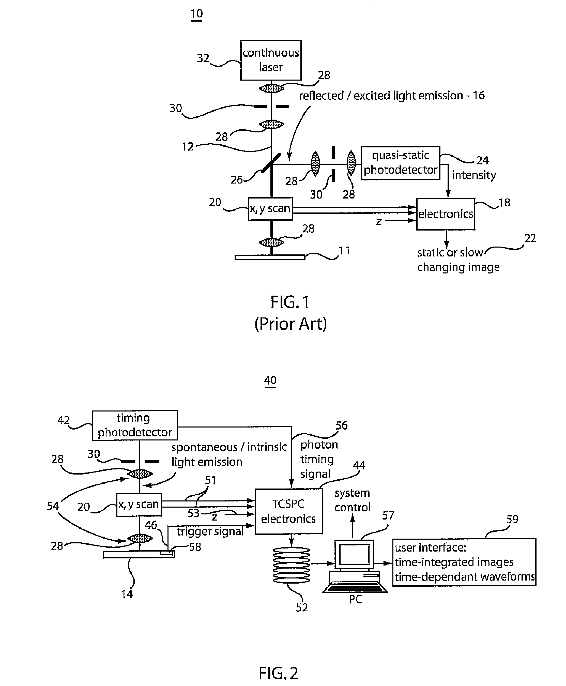
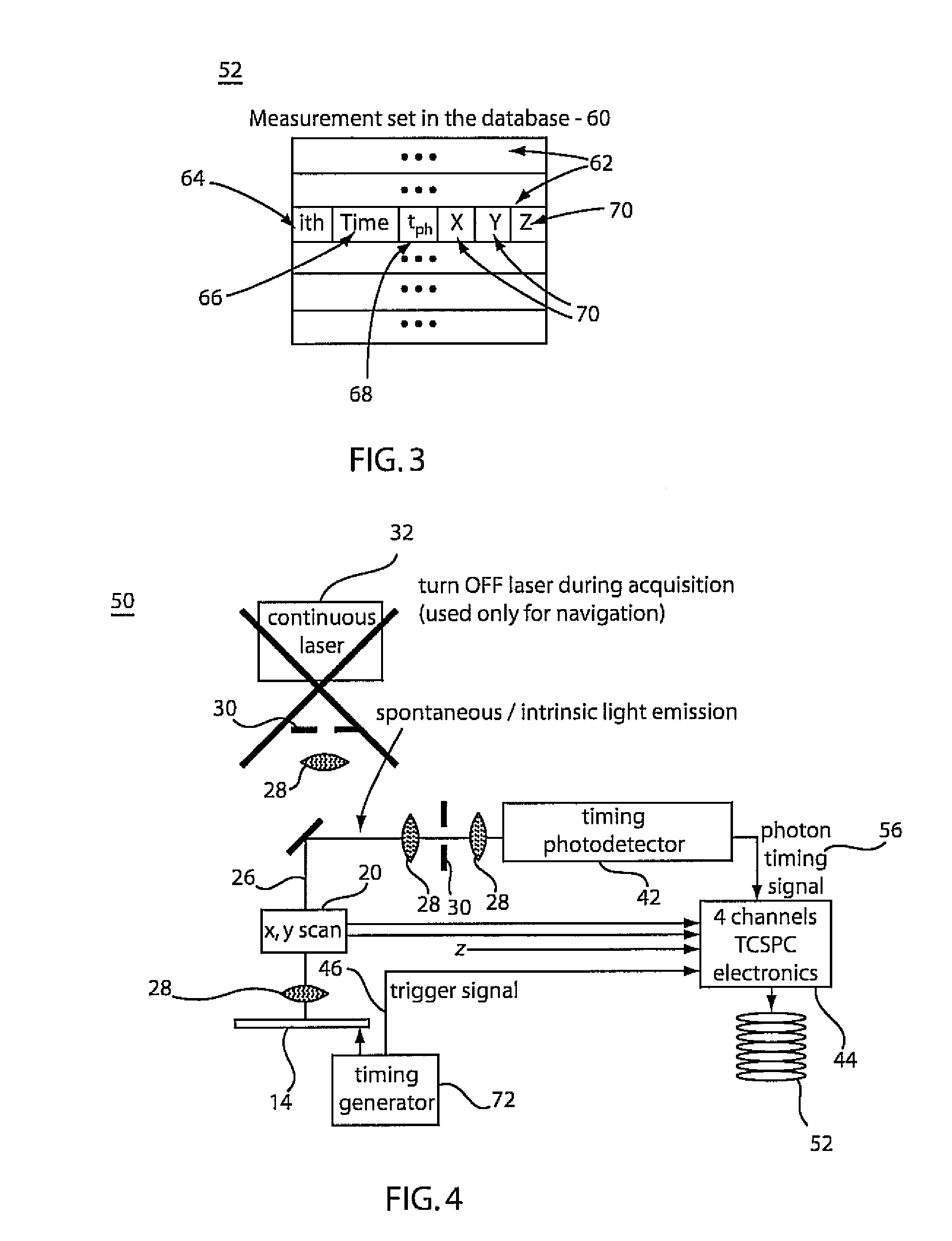
[0026]In accordance with present principles, methods and systems are presented to regain imaging capability for Picosecond Imaging for Circuit Analysis (PICA) while still using high-performance highly-optimized single pixel photodetectors. Instead of developing a photodetector with imaging capability but compromised performance, the focus is shifted to the use of single pixel photodetectors in a different optical system. This permits for the photodetector manufacturers to fully exploit the capability of their technology to maximize the single pixel performance, leaving the task of imaging to the optical system.

[0027]A single pixel or single point detector is a photodetector which is unable to spatially separate a photon inside the field of view or collection area. All the photons collected from a certain area / volume are spatially associated with a point.

[0028]Embodiments of the present invention can take the form of a hardware embodiment, or an embodiment including both hardware and...


PUM


Abstract

A Scanning Time-Resolved Emission (S-TRE) microscope or system includes an optical system configured to collect light from emissions of light generated by a device under test (DUT). A scanning system is configured to permit the emissions of light to be collected from positions across the DUT in accordance with a scan pattern. A timing photodetector is configured to detect a single photon or photons of the emissions of light from the particular positions across the DUT such that the emissions of light are correlated to the positions to create a time-dependent map of the emissions of light across the DUT.

Description

BACKGROUND[0001]1. Technical Field[0002]The present invention relates to imaging technology and more particularly to systems and methods for photon detection for use in integrated circuit analysis.[0003]2. Description of the Related Art[0004]Hot-carrier photon emission from very large scale integration (VLSI) circuits has been employed for localizing and identifying failures in circuits. With the introduction of Emission Microscopy, hot-carrier photon emission soon became an essential instrument for physical failure analysis by localizing hot-spot emission, shorts, non-uniform quiescence / stand-by current of the chip (IDDQ), etc. More advanced extensions have also been added to this technique in recent years, based, for example, on the detection of the Light Emission due to Off-State Leakage Current (LEOSLC): circuit logic states mapping, power grid drop calculation, circuit internal temperature and gate self heating measurements, etc.[0005]In 1995, the concept of Picosecond Imaging ...

Claims


Application Information

Patent Timeline
IPC IPC(8): G02B21/00G01J5/08
CPCG01J3/2803G01J3/2889G02B21/0084G01R31/307G02B21/0028G01J3/443
Inventor STELLARI, FRANCOTOSI, ALBERTOZAPPA, FRANCOSONG, PEILIN
Owner IBM CORP
Why Eureka
Try Eureka