
High power semiconductor package

a high-power semiconductor and package technology, applied in the direction of semiconductor devices, semiconductor/solid-state device details, electrical apparatus, etc., can solve the problems of poor thermal and mechanical reliability, shear stress on the interconnection pattern, deterioration of electrical and mechanical characteristics of high-power semiconductor packages, etc., to reduce the volume of the edge

Active Publication Date: 2008-07-10
SEMICON COMPONENTS IND LLC
View PDF29 Cites 44 Cited by
  • Summary
  • Abstract
  • Description
  • Claims
  • Application Information

AI Technical Summary

Benefits of technology

[0009]The present invention provides a high power semiconductor package that is designed to improve thermal resistance of the high power semiconductor to increase its lifespan.
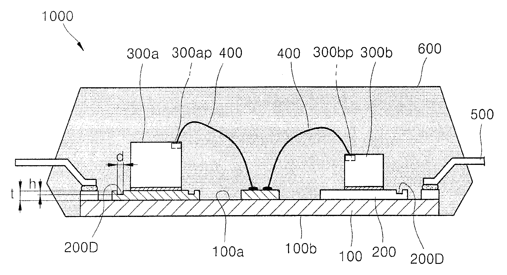
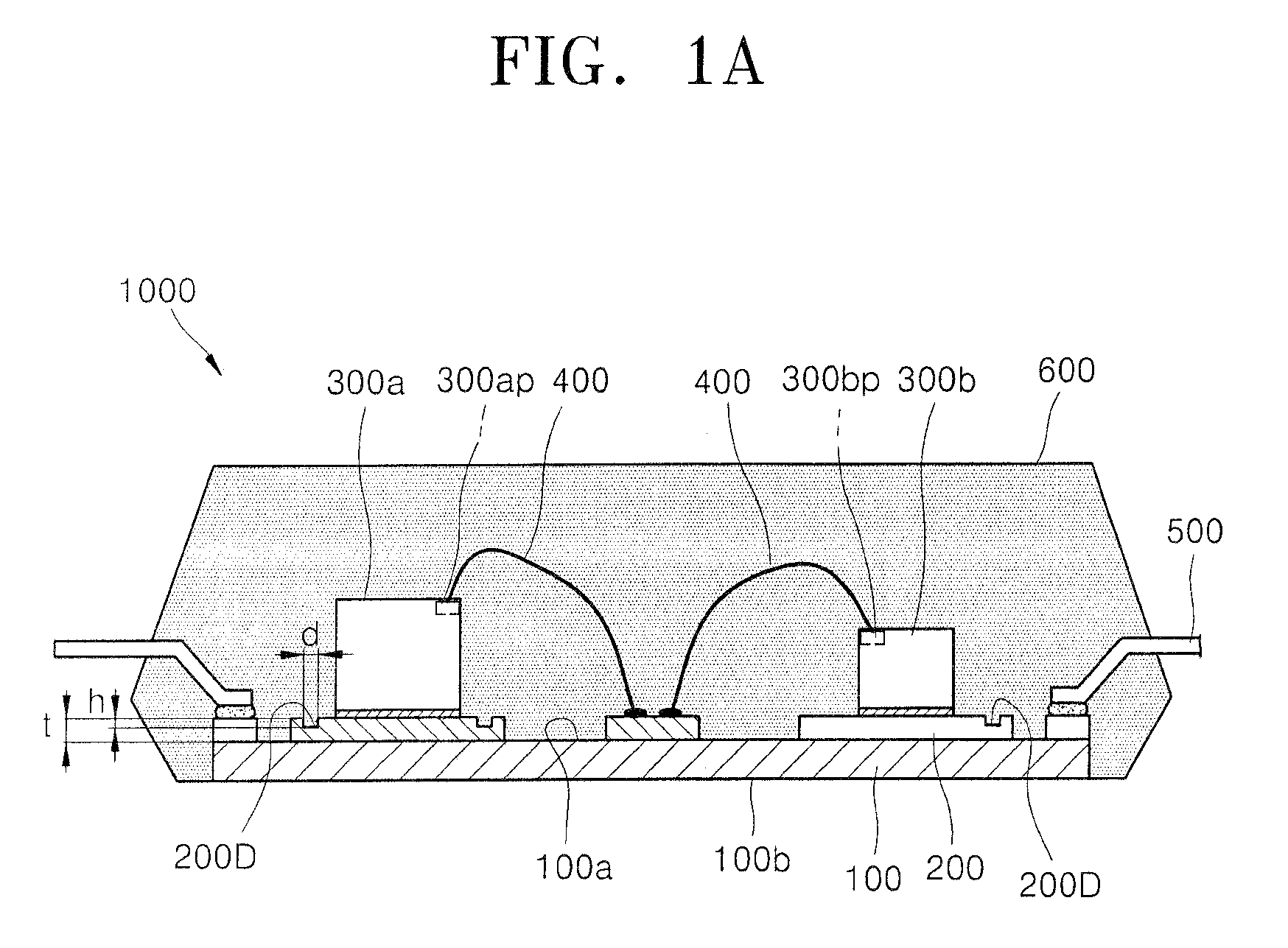
[0012]The first dimples may have a diameter in a range from 0.1 mm to 3 mm. The first dimples may range in depth from 10% to 100% of a thickness of the interconnection patterns. The first dimples may be formed in an edge of the interconnection patterns so as to reduce shear stress concentrated at the edge of the interconnection patterns.
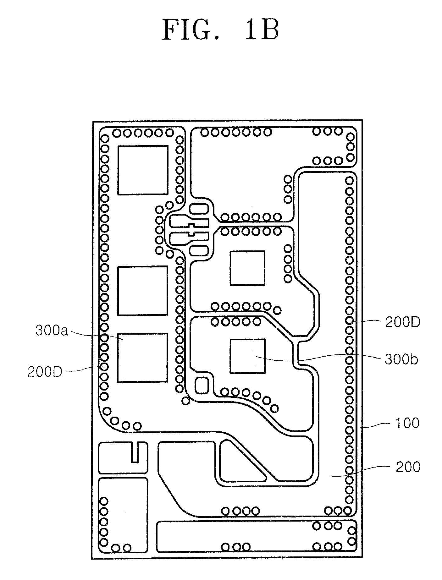
[0013]The first dimples may be arranged at regular intervals in at least one row. The first dimples may be formed in the interconnection patterns located on the edge portion of the insulation substrate more densely than in the interconnection patterns located on the center portion of the insulation substrate, so as to reduce the possibility of permeation of moisture.
[0015]The high power semiconductor package may further include a plurality of second dimples formed in an edge portion of the bottom surface of the base metal layer. The second dimples may reduce the volume of the edge of the bottom surface of the base metal layer. Therefore, the edge of the bottom surface of the base metal layer can be less deformed when the base metal layer expands by heat, and thus a shear stress caused by a difference in thermal expansion between the base metal layer and the insulation substrate can be reduced.

Problems solved by technology

Our inventors identified the cause of the poor thermal and mechanical reliability as shear stress which may result from a difference in thermal expansion coefficients of an insulating substrate and a metallic interconnection pattern.
The difference in the thermal expansion between the epoxy molding compound (EMC) and the interconnection pattern can also cause a shear stress on the interconnection pattern.
Such shear stresses can result in the delamination of the interconnection pattern from the insulating substrate, thereby deteriorating the electrical and mechanical characteristics of the high power semiconductor package and reducing the lifespan thereof.

Method used


Image

  • High power semiconductor package
  • High power semiconductor package
  • High power semiconductor package

Examples


Embodiment Construction

[0023]The present invention will now be described more fully with reference to the accompanying drawings, in which exemplary embodiments of the invention are shown.

[0024]The invention may, however, be embodied in many different forms and should not be construed as being limited to the embodiments set forth herein; rather, these embodiments are provided so that this disclosure will be thorough and complete, and will fully convey the concept of the invention to those skilled in the art. It will also be understood that when a layer is referred to as being “on” another layer or substrate, it can be directly on the other layer or substrate, or intervening layers may also be present. In the drawings, the thicknesses of layers and regions are exaggerated for clarity, and like reference numerals denote like elements. As used herein, the term “and / or” includes any and all combinations of one or more of the associated listed items.

[0025]Also, though terms like a first and a second are used to...


PUM


Abstract

Provided is a high power semiconductor package including: an insulation substrate having first and second surfaces opposite to each other; an interconnection patterns formed on the first surface of the insulation substrate, the interconnection patterns including a plurality of first dimples; a power control semiconductor chip mounted on the first surface of the insulation substrate, the power control semiconductor chip electrically connected with the interconnection patterns; and an encapsulation member encapsulating the insulation substrate, the interconnection patterns, and the power control semiconductor chip and exposing at least a portion of the second surface of the insulation substrate.

Description

CROSS-REFERENCE TO RELATED PATENT APPLICATION[0001]This application claims the benefit of Korean Patent Application No. 10-2007-0001666, filed on Jan. 5, 2007, in the Korean Intellectual Property Office, the disclosure of which is incorporated herein in its entirety by reference.BACKGROUND OF THE INVENTION[0002]1. Field of the Invention[0003]The present invention relates to a high power semiconductor package, and more particularly, to a high power semiconductor package including a power control semiconductor chip mounted on an insulation substrate.[0004]2. Description of the Related Art[0005]Power devices, such as a silicon-controlled rectifier (SCR), a power transistor, an insulated-gate bipolar transistor (IGBT) a metal oxide semiconductor (MOS) transistor, a power rectifier, a power regulator, an inverter, a converter, and a power control semiconductor chip including a combination thereof, are designed to operate in a high-voltage range from 30 V to 1000 V or higher.[0006]An insu...

Claims


Application Information

Patent Timeline
IPC IPC(8): H01L23/495
CPCH01L23/15H01L2224/45147H01L23/3735H01L23/49844H01L24/49H01L25/16H01L2224/27013H01L2224/32225H01L2224/48091H01L2224/48227H01L2224/49H01L2224/73265H01L2224/83051H01L2224/92247H01L2924/01004H01L2924/01013H01L2924/01014H01L2924/01028H01L2924/01029H01L2924/01079H01L2924/01082H01L2924/13055H01L2924/14H01L23/3107H01L2924/014H01L2924/01033H01L2924/1305H01L2924/13034H01L2924/13091H01L2224/83385H01L24/48H01L2924/01006H01L2924/01023H01L2924/00014H01L2924/00H01L2224/45015H01L2924/15787H01L2224/45124H01L2924/181H01L24/45H01L2924/00011H01L2924/2076H01L2924/00012H01L23/12
Inventor LEE, KEUN-HYUKLIM, SEUNG-WONPARK, SUNG-MINLEE, TAEK-KEUN
Owner SEMICON COMPONENTS IND LLC
Learn More