Flash memory device with hybrid structure charge trap layer and method of manufacturing same
- Summary
- Abstract
- Description
- Claims
- Application Information
AI Technical Summary
Benefits of technology
Problems solved by technology
Method used
Image
Examples
Embodiment Construction
[0025]Embodiments of the invention will now be described in some additional detail with reference to the accompanying drawings. The invention may, however, be embodied in many different forms and should not be construed as being limited to only the illustrated embodiments. Rather, these embodiments are presented as teaching examples. Throughout the drawings, the relative thickness of various layers and regions may have been exaggerated for clarity of illustration. Throughout the written description and drawings, like reference numbers are used to indicate like or similar elements, layers, and regions.
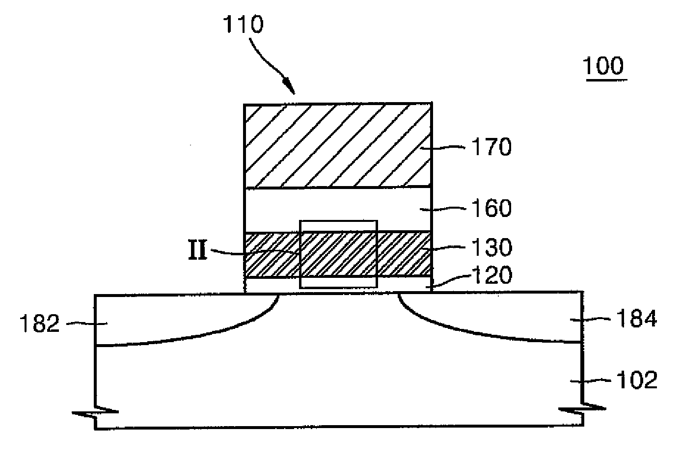
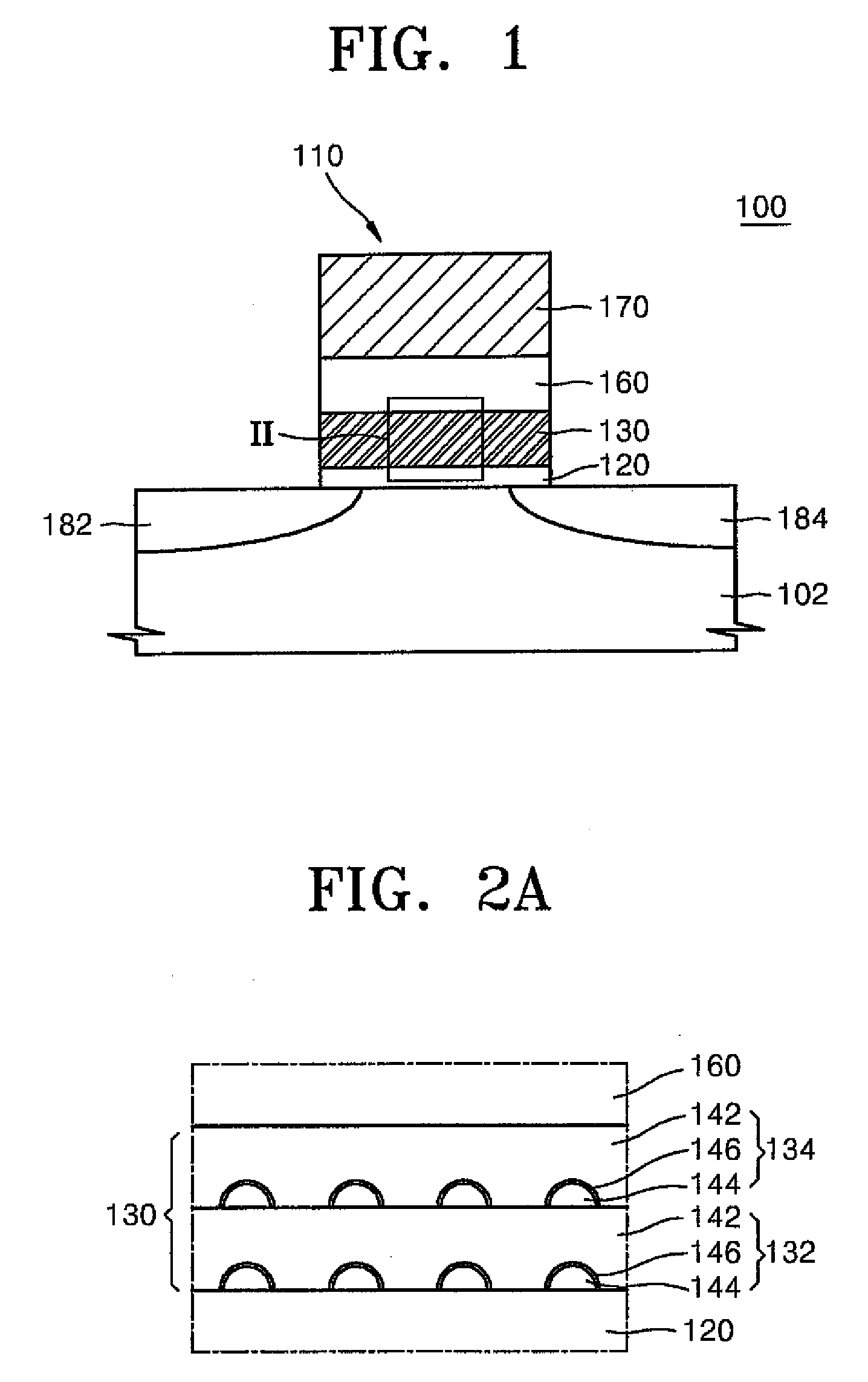
[0026]FIG. (FIG.) 1 is a sectional view illustrating a portion of a flash memory device 100 according to an embodiment of the invention.
[0027]Referring to FIG. 1, the flash memory device 100 includes a gate stack structure 110 formed on a semiconductor substrate 102. The gate stack structure 110 includes a tunneling insulating layer 120 formed on the semiconductor substrate 102, a charg...
PUM
 Abstract
Description
Claims
Application Information


