Interconnects containing bilayer porous low-k dielectrics using different porogen to structure former ratio

a low-k dielectric and bilayer porous technology, applied in the direction of nuclear engineering, transportation and packaging, railway signalling, etc., can solve the problems of poor device reliability and poor device performance, and achieve the effects of improving dielectric hardness, reducing processing costs, and precise and uniform control of metal conductor resistan

Inactive Publication Date: 2008-07-17
TAIWAN SEMICON MFG CO LTD
View PDF34 Cites 58 Cited by
  • Summary
  • Abstract
  • Description
  • Claims
  • Application Information

AI Technical Summary

Benefits of technology

[0008]The bilayer porous low-k dielectric interconnect structure of this invention offers better physical and chemical strength in the dielectric layer by achieving desired pore size, pore density and desired dielectric hardness via fine-tuning PECVD processing parameters and curing parameters afterwards. The improved dielectric hardness leads to more controllable etching rate and better trench / via bottom roughness, which in turn, result in better barrier layer adhesion in preventing Cu diffusion and better Cu / TaN / LK interface and reduced inter-metal layer capacitance. The improved dielectric hardness also enables the top dielectric layer to be used as a CMP polish stop layer. The avoidance of a dedicated CMP polish stop layer leads to reduction of processing costs.
[0029]The method of forming the interconnect structure of this invention results in different dielectric properties (k value and material hardness) in the bilayer dielectrics, which enables the bottom dielectric layer to serve as an inherent etch stop layer for the top dielectric layer during trench etch, which, in turn, leads to precise and uniform control over metal conductor resistance without thickness variation of the metal conductors. Furthermore, the avoidance of a dedicated buried etch stop layer leads to reduction of processing costs.

Problems solved by technology

The first aspect of this invention provides an inventive interconnect structure aimed to solve or circumvent the problems in the prior art, which cause poor device performance and poor device reliability.

Method used


Image

  • Interconnects containing bilayer porous low-k dielectrics using different porogen to structure former ratio
  • Interconnects containing bilayer porous low-k dielectrics using different porogen to structure former ratio
  • Interconnects containing bilayer porous low-k dielectrics using different porogen to structure former ratio

Examples


Embodiment Construction

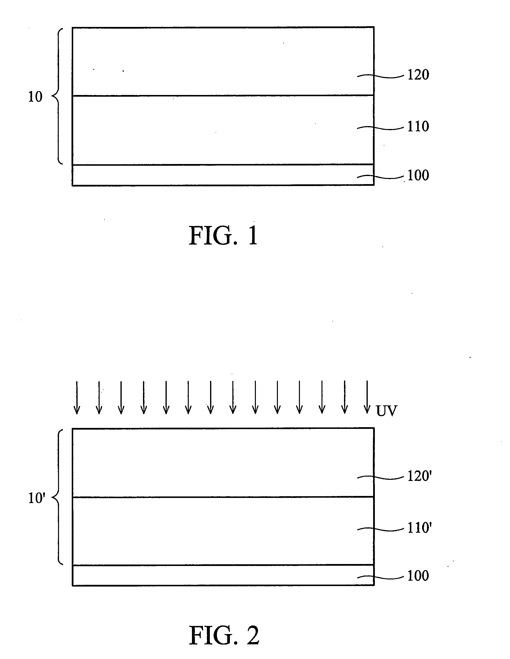
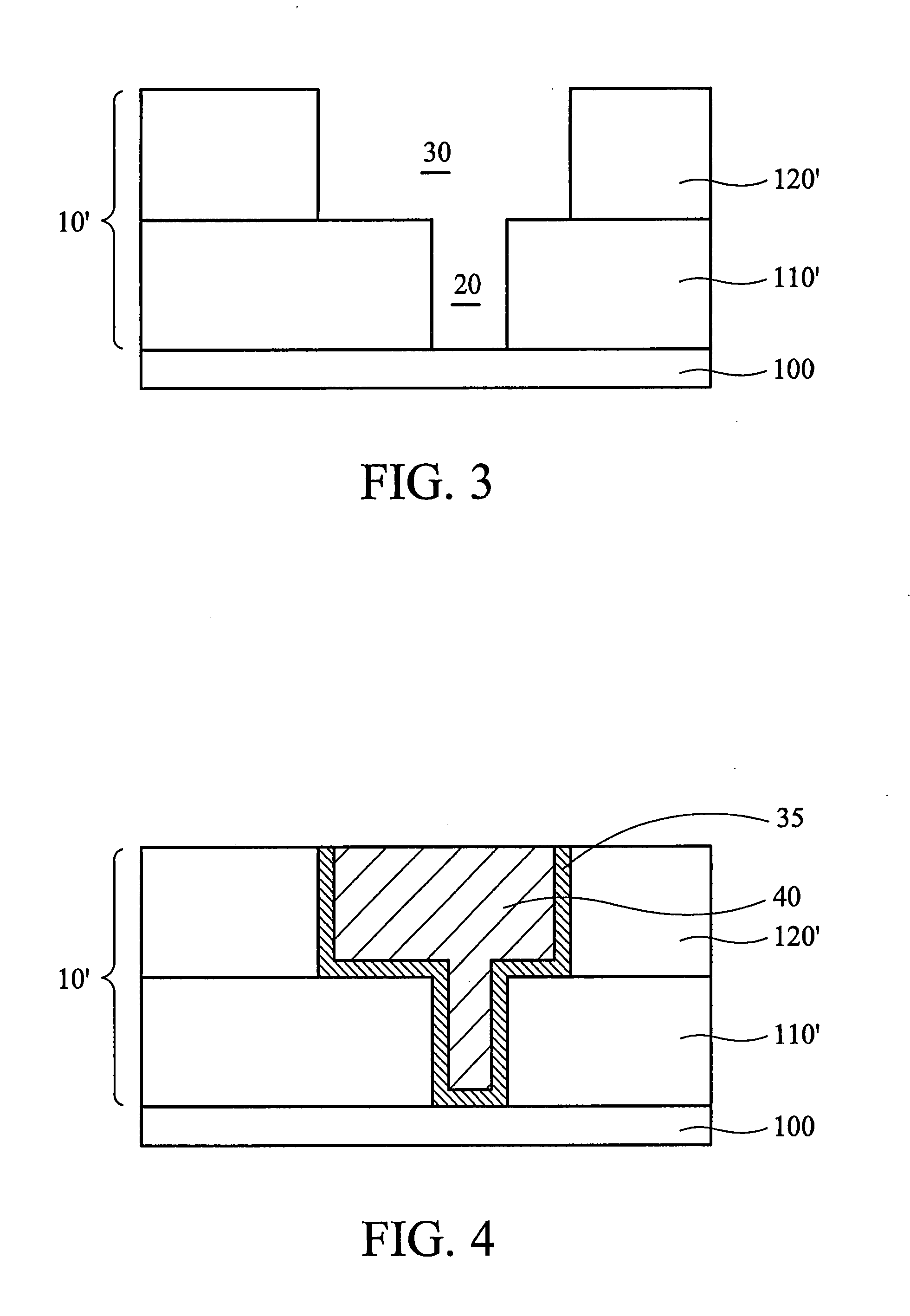
[0036]The making and using of the presently preferred embodiments are discussed in detail below. It should be appreciated, however, that the present invention provides many applicable inventive concepts that can be embodied in a wide variety of specific contexts. The specific embodiments discussed are merely illustrative of specific ways to make and use the invention, and do not limit the scope of the invention.

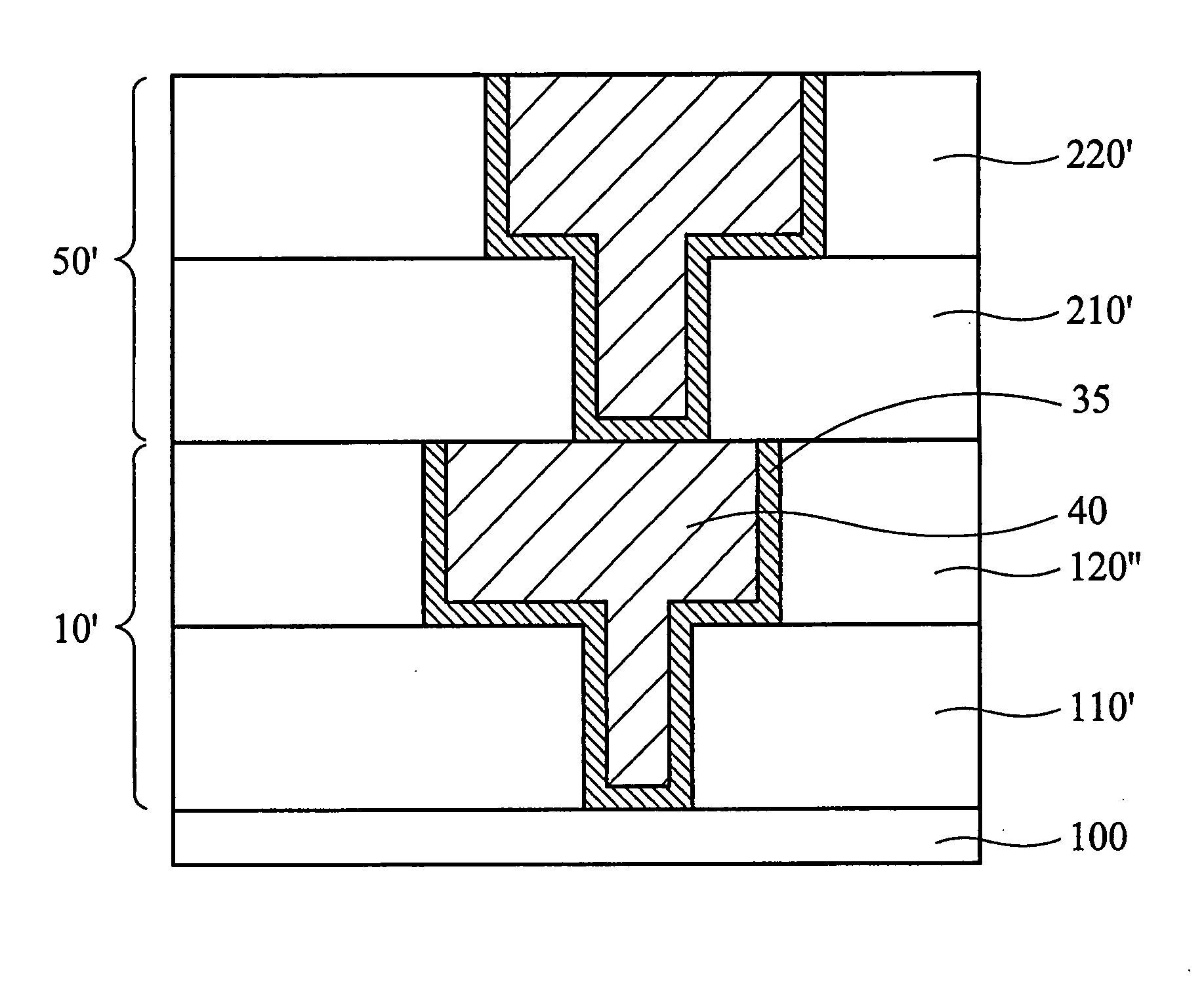
[0037]It is believed that the embodiments of this invention are particularly advantageous in low-k dual damascene (DD) interconnect structures. Advantageous features of the embodiments may include good physical and chemical strength on inter-metal layer low-k dielectrics, lower intra-metal capacitance due to lower k of intra-metal dielectrics, improved control on inter-metal layer dielectric constant and hardness, better trench / via bottom roughness, precise and uniform control over trench depth, lower k damage during trench etching, avoidance of the need for a buried etch sto...


PUM

PropertyMeasurementUnit
dielectric constantaaaaaaaaaa
dielectric constantsaaaaaaaaaa
temperatureaaaaaaaaaa

Abstract

A bilayer porous low dielectric constant (low-k) interconnect structure and methods of fabricating the same are presented. A preferred embodiment having an effective dielectric constant of about 2.2 comprises a bottom deposited dielectric layer and a top deposited dielectric layer in direct contact with the former. The bottom layer and the top layer have same atomic compositions, but a higher dielectric constant value k. The bottom dielectric layer serves as an etch stop layer for the top dielectric layer, and the top dielectric layer can act as CMP stop layer. One embodiment of making the structure includes forming a bottom dielectric layer having a first porogen content and a top dielectric layer having a higher porogen content. A curing process leaves lower pore density in the bottom dielectric layer than that left in the top dielectric layer, which leads to higher dielectric value k in the bottom dielectric layer.

Description

TECHNICAL FIELD[0001]The present invention relates generally to interconnect structures for high speed and reliable electronic signal transmission in very large scale semiconductor integrated circuits (VLSI) and more particularly to bilayer porous low dielectric constant (low-k) interconnect structures and methods of fabricating the same.BACKGROUND[0002]Low-k dielectric material plus copper (Cu) dual damascene interconnect structures are well known to those skilled in the semiconductor art to be the choice for high speed and reliable signal transmission in VLSI, particularly as device feature sizes on an IC continue to scale down. While having extremely low-k value to significantly reduce inter / intra-metal layer capacitance, which in turn reduces signal RC delays and enhance signal integrity, porous low-k (PLK) dielectric materials have been facing some major technical obstacles to be fully integrated into existing IC manufacturing processes. Among those obstacles are poor control o...

Claims


Application Information

Patent Timeline
Patent Type & Authority Applications(United States)
IPC IPC(8): H01L21/4763
CPCH01L21/76807H01L21/7682H01L21/76835H01L23/53295H01L23/53238H01L23/5329H01L23/53223H01L2924/0002H01L2924/00
Inventor YU, CHEN-HUALU, YUNG-CHENGJENG, PEI-RENCHOU, CHIA-CHENGLIN, KENG-CHUKO, CHUNG-CHIBAO, TIEN-IJENG, SHWANG-MING
Owner TAIWAN SEMICON MFG CO LTD
Why Eureka
Try Eureka