
Hybrid process for forming metal gates

a metal oxide and hybrid technology, applied in the direction of semiconductors, semiconductor devices, electrical equipment, etc., can solve the problems of increasing the effective gate dielectric thickness, affecting the efficiency of pmos devices, so as to prevent the work function shift of pmos devices and improve the carrier depletion

Inactive Publication Date: 2008-07-24
TAIWAN SEMICON MFG CO LTD
View PDF11 Cites 56 Cited by
  • Summary
  • Abstract
  • Description
  • Claims
  • Application Information

AI Technical Summary

Benefits of technology

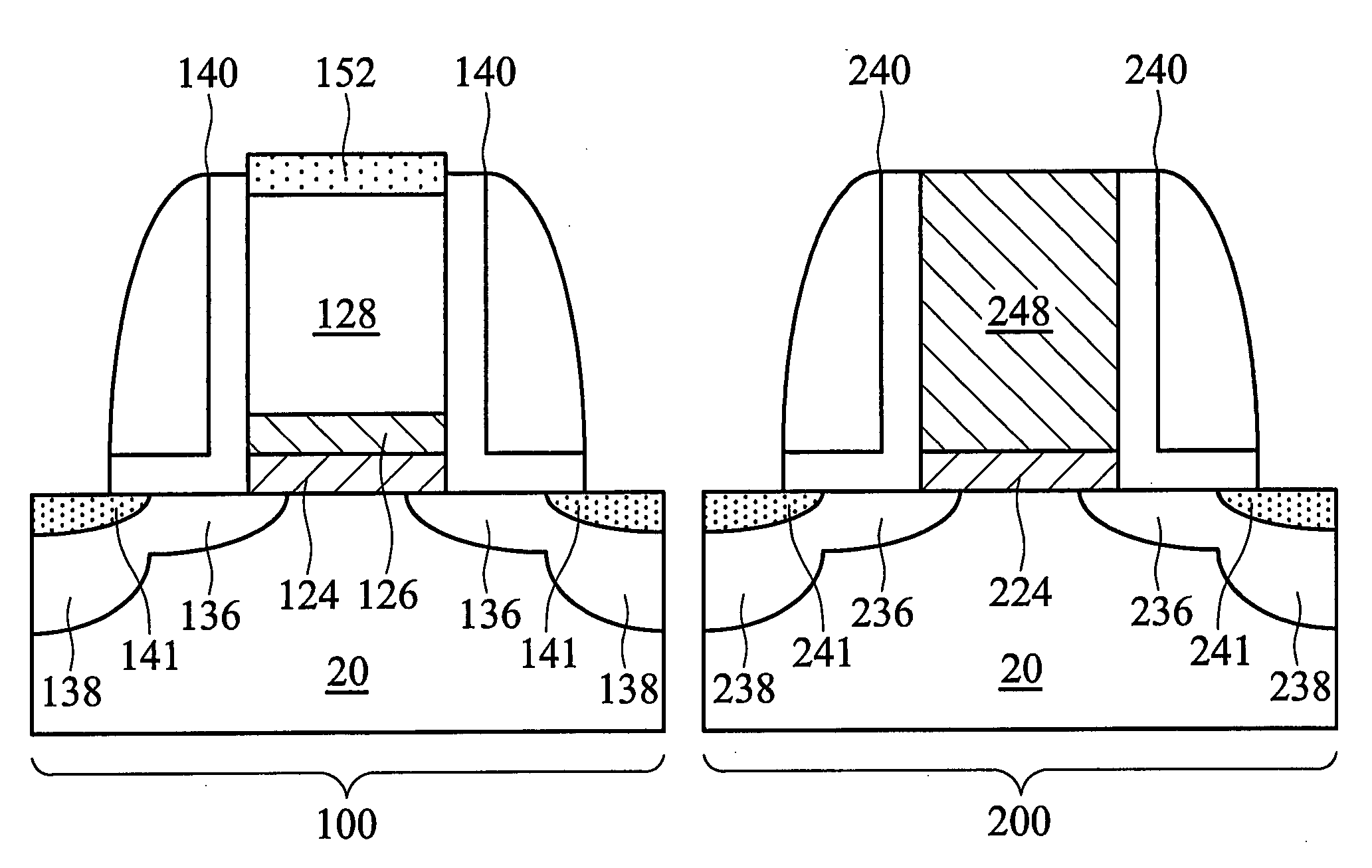
The present invention provides a semiconductor structure that includes both NMOS and PMOS devices, which prevents work function shift of PMOS devices without increasing manufacturing costs or degrading stresses. The structure includes a semiconductor substrate, a first MOS device with a first gate dielectric and a first metal-containing gate electrode layer, a first contact etch stop layer, a first region between the first contact etch stop layer and the first metal-containing gate electrode layer, a second MOS device with a second gate dielectric and a second metal-containing gate electrode layer, and a second contact etch stop layer. The structure also includes a method for forming the semiconductor structure with the NMOS and PMOS devices. The technical effects of the invention include preventing work function shift of PMOS devices and improving the performance of semiconductor devices.

Problems solved by technology

The depletion effect results in an increase in the effective gate dielectric thickness, making it more difficult for an inversion layer to be created at the surface of the semiconductor.
The use of thin gate dielectrics tends to make the carrier depletion effect worse.
With thin gate dielectrics, the depletion layer in the polysilicon gate becomes more significant in thickness when compared to the thickness of the thin gate dielectrics, and thus device performance degradation worsens.
As a result, the carrier depletion effect in the gate electrodes limits device scalability by imposing a lower bound on how much the effective gate dielectric thickness can be reduced.
However, for PMOS devices, even though metallic materials having band-edge work functions have been found, these materials have poor thermal stability.
The performance of the resulting PMOS devices is thus adversely affected.
Both approaches have advantageous and disadvantageous features.
However, since the metal gates are formed before the formation and the activation of LDD regions and source / drain regions, they suffer from high thermal budgets, and the work functions of PMOS devices may shift.
In addition, patterning metal layers by etching is relatively difficult.
However, the process is complex.
This results in the significant degradation in the contact etch stop layers' ability of applying stresses.

Method used


Image

  • Hybrid process for forming metal gates
  • Hybrid process for forming metal gates
  • Hybrid process for forming metal gates

Examples


Embodiment Construction

[0017]The making and using of the presently preferred embodiments are discussed in detail below. It should be appreciated, however, that the present invention provides many applicable inventive concepts that can be embodied in a wide variety of specific contexts. The specific embodiments discussed are merely illustrative of specific ways to make and use the invention, and do not limit the scope of the invention.

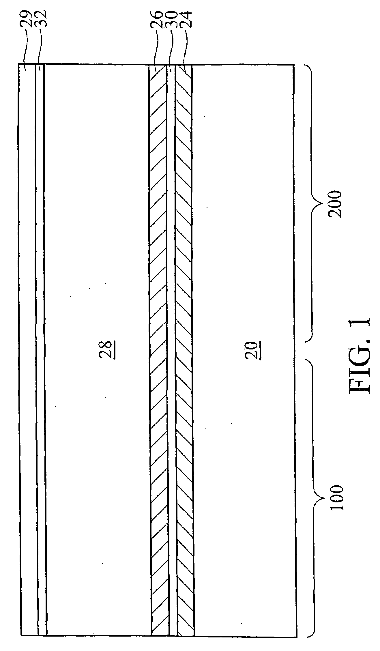
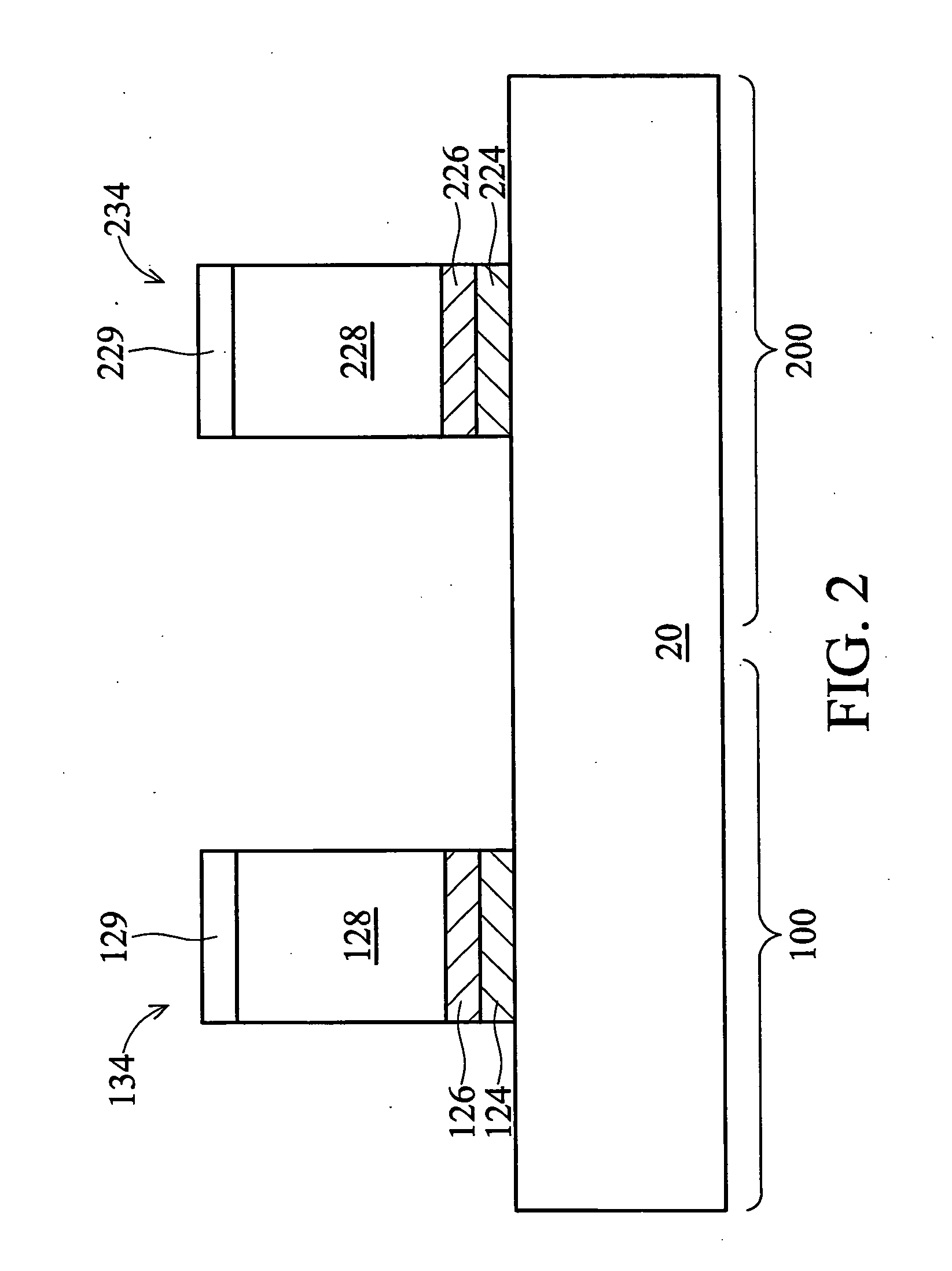
[0018]A hybrid method for forming complementary metal-oxide-semiconductor (CMOS) devices with dual metal gates is provided. The hybrid method combines gate-first and gate-last approaches to achieve better effects. The intermediate stages of manufacturing a preferred embodiment of the present invention are illustrated. Throughout the various views and illustrative embodiments of the present invention, like reference numbers are used to designate like elements.

[0019]Referring to FIG. 1, substrate 20 is provided, which may be formed of commonly used semiconductor materials and s...


PUM


Abstract

A semiconductor structure and methods for forming the same are provided. The semiconductor structure includes a first MOS device of a first conductivity type and a second MOS device of a second conductivity type opposite the first conductivity type. The first MOS device includes a first gate dielectric on a semiconductor substrate; a first metal-containing gate electrode layer over the first gate dielectric; and a silicide layer over the first metal-containing gate electrode layer. The second MOS device includes a second gate dielectric on the semiconductor substrate; a second metal-containing gate electrode layer over the second gate dielectric; and a contact etch stop layer having a portion over the second metal-containing gate electrode layer, wherein a region between the portion of the contact etch stop layer and the second metal-containing gate electrode layer is substantially free from silicon.

Description

TECHNICAL FIELD[0001]This invention relates generally to semiconductor devices, and more particularly to structures of metal-oxide-semiconductor (MOS) devices and manufacturing methods for forming the same.BACKGROUND[0002]Metal-oxide-semiconductor (MOS) devices are basic building elements in integrated circuits. A conventional MOS device typically has a gate electrode comprising polysilicon doped with p-type or n-type impurities, using doping operations such as ion implantation or thermal diffusion. It is preferred to adjust the work function of the gate electrode to the band-edge of the silicon; that is, for an NMOS device, adjusting the work function close to the conduction band, and for a PMOS device, adjusting the work function close to the valence band. Adjusting the work function of the polysilicon gate electrode can be achieved by selecting appropriate impurities.[0003]MOS devices with polysilicon gate electrodes exhibit carrier depletion effect, which is also referred to as ...

Claims


Application Information

Patent Timeline
Patent Type & Authority Applications(United States)
IPC IPC(8): H01L27/092
CPCH01L21/28044H01L21/28088H01L21/823835H01L29/7843H01L29/66545H01L29/6656H01L29/7833H01L21/823842
Inventor HOU, YONG-TIANHSU, PENG-FUYING, JINLIN, KANG-CHENGHUANG, K. T.LEE, TZE-LIANG
Owner TAIWAN SEMICON MFG CO LTD
Learn More