Methods of forming silicon nanocrystals by laser annealing

a technology of silicon nanocrystals and laser annealing, which is applied in the direction of crystal growth process, polycrystalline material growth, chemically reactive gas growth, etc., can solve the problems of reducing the height of pl intensity, limiting the application of pl devices, and low quantum efficiency of sro materials, so as to achieve enhanced chemical vapor deposition

Active Publication Date: 2008-07-31
AU OPTRONICS CORP
View PDF37 Cites 31 Cited by
  • Summary
  • Abstract
  • Description
  • Claims
  • Application Information

AI Technical Summary

Benefits of technology

[0017]The silicon-rich dielectric layer can be formed by using a plasma enhanced chemical vapor deposition (PECVD) process at a process temperature effective in the range of about 200° C. to 400° C., and a process time effective in a duration of about 13 seconds to 250 seconds to form a corresponding thickness in the range of about 50 nm to 1000 nm. The silicon content ratio SiH4 / N2O of the silicon-rich dielectric layer is adjustable to form the silicon-rich dielectric layer with a desired refractive index. In one embodiment, the silicon content ratio SiH4 / N2O is changeable in the range of about 1:10 to 1:1, resulting in a refractive index of the silicon-rich dielectric layer to be at least in the range of about 1.4 to 2.3, respectively.

Problems solved by technology

However, these SRO materials exhibit low quantum efficiency and have a stability problem, which reduces the PL intensity height over time, and limits their application to PL devices.
However, state-of-the-art implantation processes have not been able to distribute the dopant uniformly, which lowers the light emitting efficiency and increases costs.
At the same time, there has been no interface engineering sufficient to support the use of such a dopant.
Using the Si / SiO2 superlattice structure to control crystal size results in a slow, high-temperature deposition process that cannot simultaneously control both the Si particle size and the quality Si nanocrystal / SiO2 interface.
The device efficiency is very low, which limits the device applications.
Scaling the tunnel oxide leads to anomalous charge leakage, caused by one or two defects in the oxide.
Such a leakage causes the information stored in the non-volatile memory to be lost.
Scaling the tunnel oxide also requires high operating voltage.
However, due to aforementioned manufacturing difficulties, these materials are not easily integrated in the conventional manufacturing process.
Therefore, it is apparent that a heretofore unaddressed need exists in the art to address the aforementioned deficiencies and inadequacies.

Method used


Image

  • Methods of forming silicon nanocrystals by laser annealing
  • Methods of forming silicon nanocrystals by laser annealing
  • Methods of forming silicon nanocrystals by laser annealing

Examples


Embodiment Construction

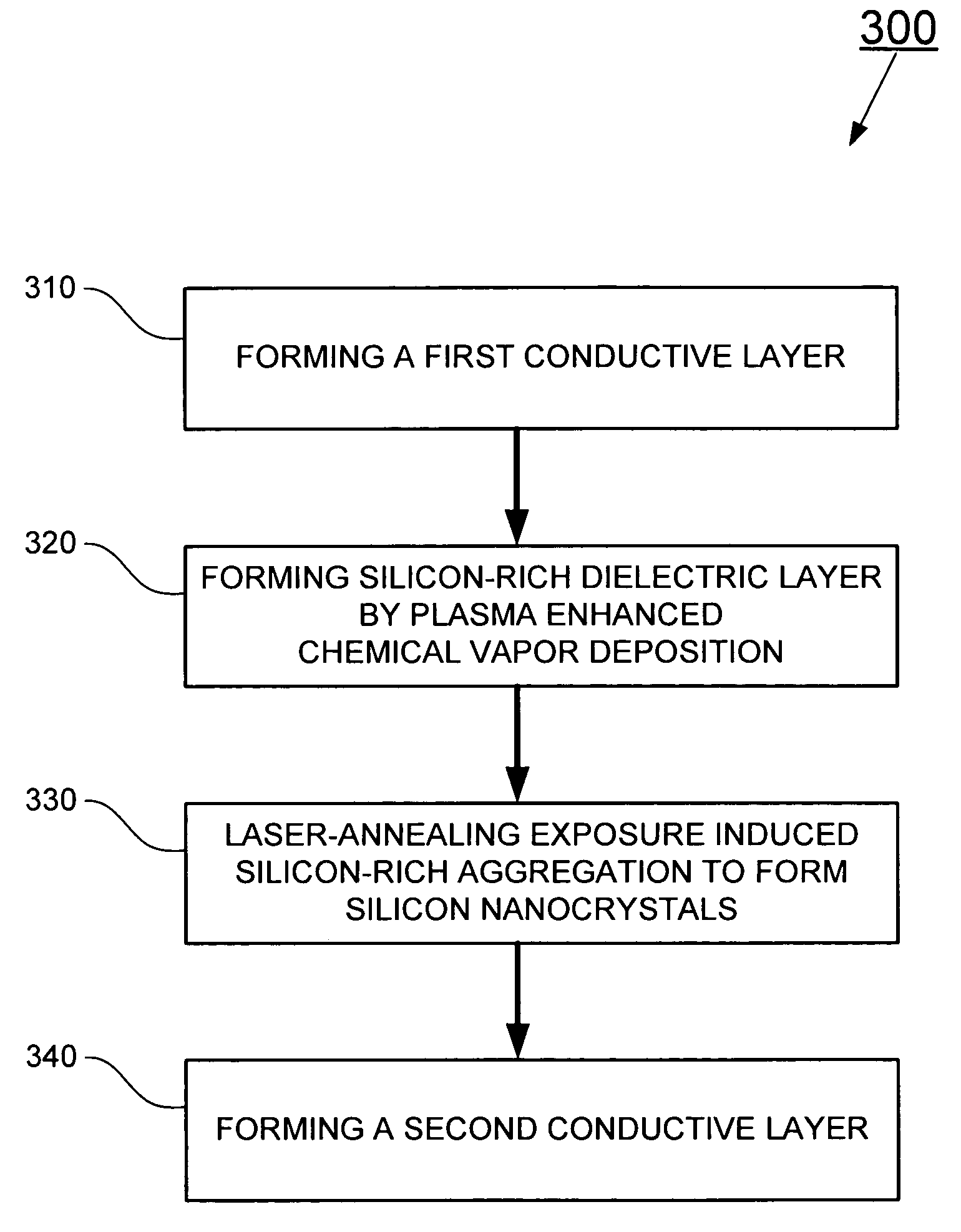
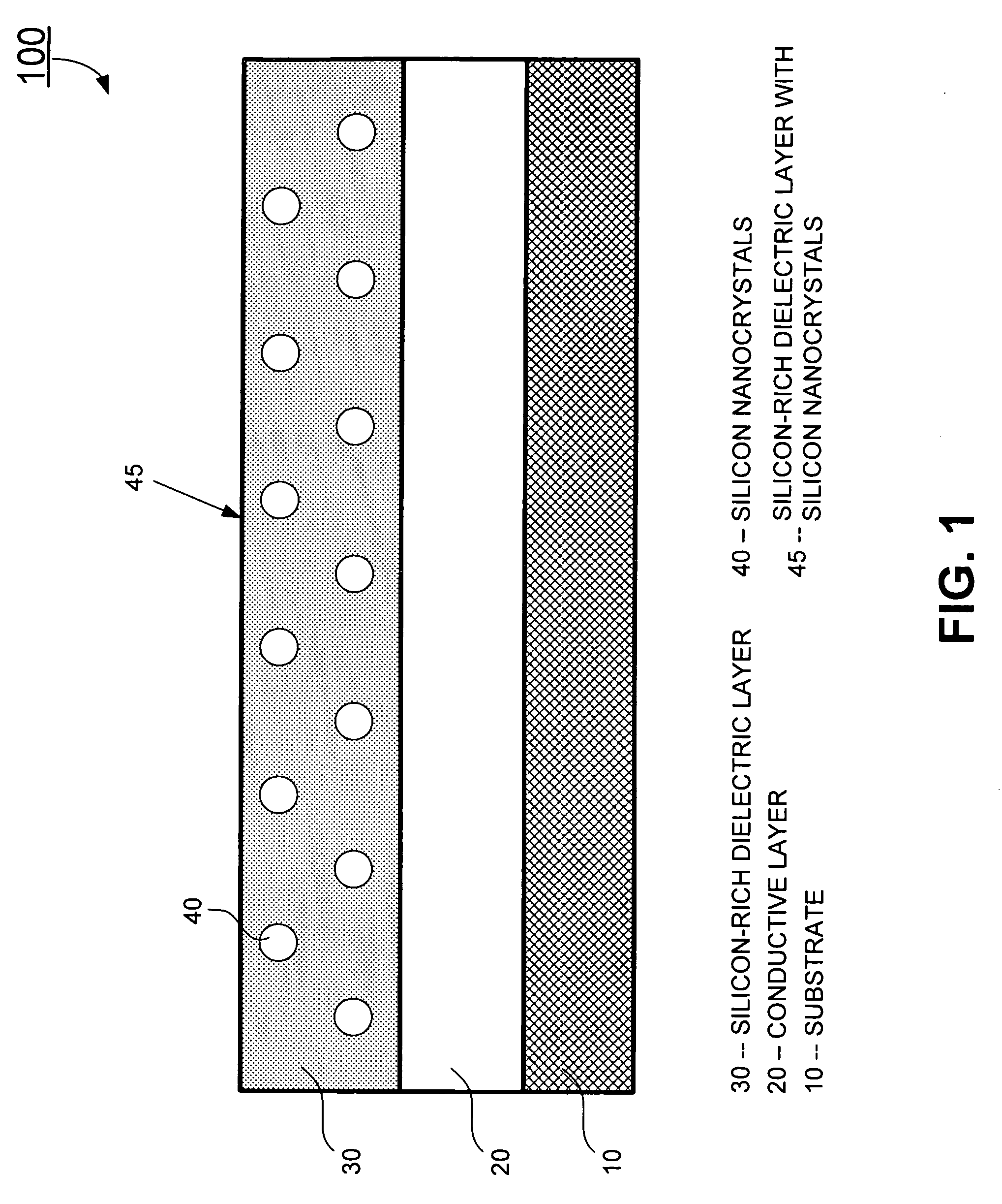
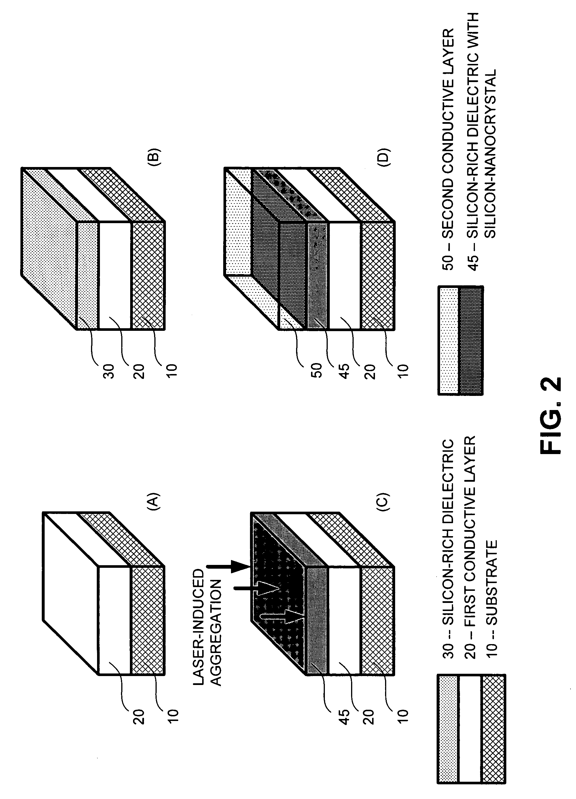
[0029]The present invention is more particularly described in the following examples that are intended as illustrative only since numerous modifications and variations therein will be apparent to those skilled in the art. Various embodiments of the invention are now described in detail. Referring to the drawings, like numbers indicate like components throughout the views. As used in the description herein and throughout the claims that follow, the meaning of “a”, “an”, and “the” includes plural reference unless the context clearly dictates otherwise. Also, as used in the description herein and throughout the claims that follow, the meaning of “in” includes “in” and “on” unless the context clearly dictates otherwise.

[0030]The terms used in this specification generally have their ordinary meanings in the art, within the context of the invention, and in the specific context where each term is used.

[0031]Certain terms that are used to describe the invention are discussed below, or elsew...


PUM

PropertyMeasurementUnit
refractive indexaaaaaaaaaa
thicknessaaaaaaaaaa
temperatureaaaaaaaaaa

Abstract

The present invention relates to a method for forming a layered structure with silicon nanocrystals. In one embodiment, the method comprises the steps of: (i) forming a first conductive layer on a substrate, (ii) forming a silicon-rich dielectric layer on the first conductive layer, and (iii) laser-annealing at least the silicon-rich dielectric layer to induce silicon-rich aggregation to form a plurality of silicon nanocrystals in the silicon-rich dielectric layer. The silicon-rich dielectric layer is one of a silicon-rich oxide film having a refractive index in the range of about 1.4 to 2.3, or a silicon-rich nitride film having a refractive index in the range of about 1.7 to 2.3. The layered structure with silicon nanocrystals in a silicon-rich dielectric layer is usable in a solar cell, a photodetector, a touch panel, a non-volatile memory device as storage node, and a liquid crystal display.

Description

FIELD OF THE INVENTION[0001]The present invention relates generally to a method of forming silicon nanocrystals by laser annealing upon a silicon-rich dielectric film.BACKGROUND OF THE INVENTION[0002]Photoluminescence (PL) devices find their applications in many areas such as solar cells, touch panels, UV-Blue photodetectors, as well as full-color, high quality TFT flat panel display. Such photoluminescence devices may be fabricated with nanocrystals. Traditionally, semiconductor materials such as Si, Ge are used to produce nanocrystals based on the concepts of band gap and quantum confinement effects of these materials. Exemplary PL devices are disclosed in published U.S. Patent Application 2006 / 0189014, which is incorporated herein in its entirety by reference for background information only. One widely-used method of fabricating silicon nanocluster is to precipitate the silicon nanocluster out of SiOx (where x<2), producing a film using chemical vapor deposition, radio frequen...

Claims


Application Information

Patent Timeline
Patent Type & Authority Applications(United States)
IPC IPC(8): C03B25/00
CPCC23C16/345C23C16/56C23C16/401Y10S977/891Y10S977/784Y10S977/89Y10S977/809Y10S977/844Y10S977/814
Inventor CHO, AN-THUNGCHAO, CHIH-WEIPENG, CHIA-TIENLIU, WAN-YISUN, MING-WEI
Owner AU OPTRONICS CORP
Why Eureka
Try Eureka