Contact Probe And Socket For Testing Semiconductor Chips

a contact probe and semiconductor chip technology, applied in the field of contact probes, can solve the problems of reducing test reliability, contact resistance, and the limitation of the method of providing elastic force to the test contact probe using the elastic spring, and achieves the effect of reducing signal path, simple structure and easy manufacturing

Inactive Publication Date: 2008-07-31
LEENO IND INC
View PDF9 Cites 14 Cited by
  • Summary
  • Abstract
  • Description
  • Claims
  • Application Information

AI Technical Summary

Benefits of technology

[0016]Accordingly, the present invention has been made keeping in mind the above problems occurring in the prior art, and an object of the present invention is to provide a contact probe and socket for testing semiconductor chips, which employs a simple structure that is easily manufactured, and reduces a signal path, thus improving test reliability.
[0017]Another object of the present invention is to provide a contact probe for testing semiconductor chips, in which the dimensions of test equipment are remarkably reduced.

Problems solved by technology

However, this conventional contact probe has various problems in that the contact resistance thereof is great because electric current applied to the probe needle flows through the contact area between the outer case and the spring, in that the elastic force of the spring is reduced by over-current, and in that a signal path of the applied current is increased, thus reducing test reliability.
Therefore, the method of providing the elastic force to the test contact probe using the elastic spring has reached a limitation.
However, these conventional technologies are unsuitable for miniaturization required for the test equipment of a highly integrated circuit resulting from technical development, and make the production and assembly of each element difficult due to structural complexity thereof.

Method used


Image

  • Contact Probe And Socket For Testing Semiconductor Chips
  • Contact Probe And Socket For Testing Semiconductor Chips
  • Contact Probe And Socket For Testing Semiconductor Chips

Examples


Embodiment Construction

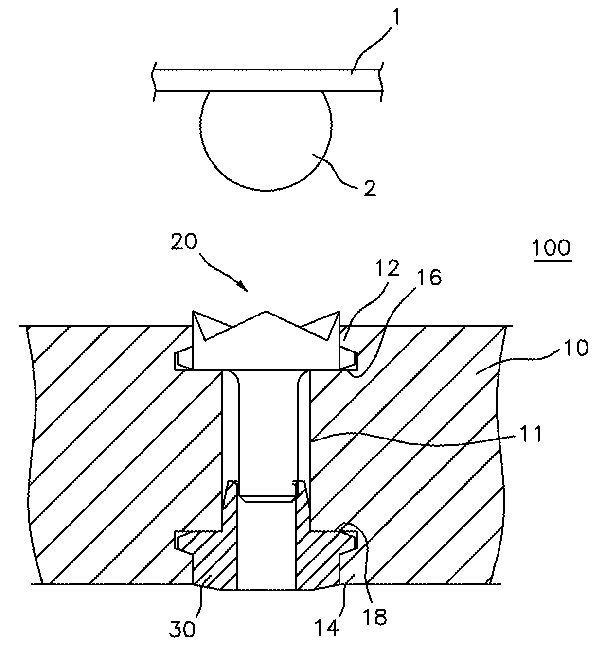
[0041]A contact probe and socket for testing semiconductor chips according to an exemplary embodiment of the invention will now be described in greater detail with reference to the accompanying drawings.

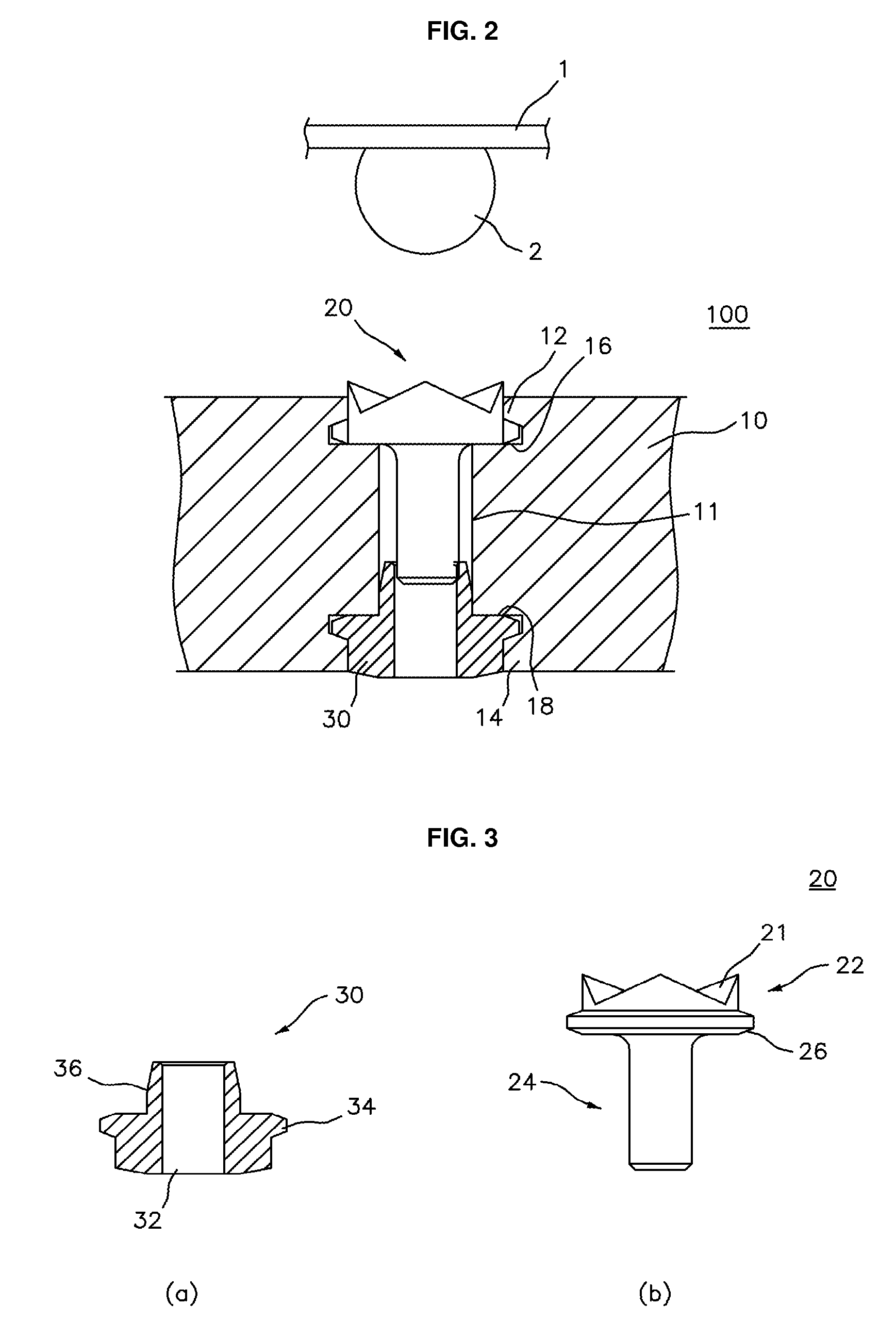
[0042]FIG. 2 is a sectional view illustrating a contact probe for testing semiconductor chips according to an exemplary embodiment of the invention. FIG. 3 illustrates a plunger and a contact pin according to an exemplary embodiment of the invention, in which FIG. 3(a) is a sectional view of the plunger, and FIG. 3(b) is a front view of the contact pin.

[0043]FIGS. 4 and 5 are a perspective view and a front view illustrating a contact socket for testing semiconductor chips according to an exemplary embodiment of the invention, respectively. FIG. 6 is a plan view illustrating an elastic plate, part of which is enlarged, according to an exemplary embodiment of the invention.

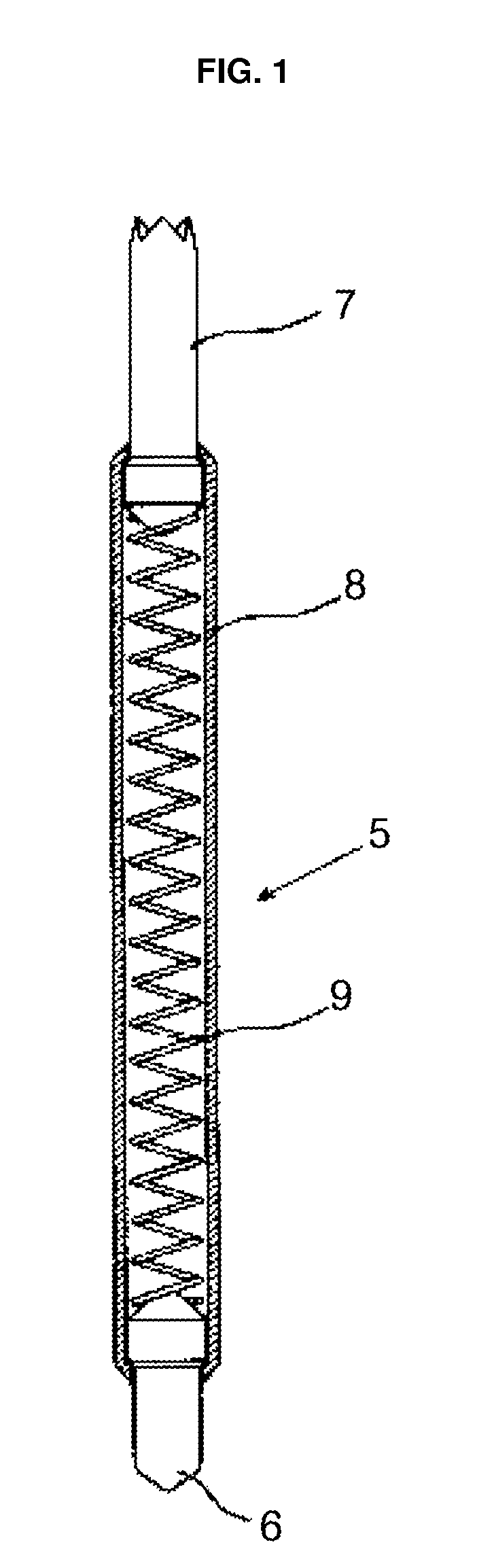
[0044]As illustrated in FIG. 2, the contact probe for testing semiconductor chips comprises plungers 20 brought in...


PUM


Abstract

A contact probe and a socket for testing semiconductor chips are provided with a simple structure, so that they can be easily manufactured, and can reduce a signal path not only to improve test reliability but also remarkably reduce the dimensions of test equipment. The contact probe comprises: a nonconductive elastic plate having main through-holes corresponding to contact terminals of a test target; plungers coupled on upper sides of the main through-holes, each having a plunger head that is elastically supported by the elastic plate and a plunger body that extends downwards from the center of the plunger head; and contact pins coupled on lower sides of the main through-holes, each having a receiving hole contacting the plunger body of each plunger at a center thereof. Thus, the contact probe employs a simple structure capable of coupling the plungers to the nonconductive elastic plate and elastically supporting the plungers, so that they can be easily manufactured, improve the signal pass of test electric current to secure test reliability, and be manufactured at a subminiature size suitable for equipment for testing semiconductor chips, which are gradually becoming complicated due to technical development.

Description

FIELD OF THE INVENTION[0001]The present invention relates to a contact probe, and more particularly to a contact probe and a socket for testing semiconductor chips, in which each plunger is coupled to an elastic plate made of nonconductive material.BACKGROUND OF THE INVENTION[0002]A chip is an integrated circuit that performs a variety of functions using logic elements fabricated on a thin small piece of semiconducting material, such functions being activated by electrical signals transmitted from a printed circuit board (PCB) through buses.[0003]In general, a lot of chips are mounted in a variety of electronic products, and play an important role in determining the performance of each electronic product.[0004]Further, the PCB is constructed so that a conductor, copper, is coated on a thin board made of an insulator, such as epoxy resin or bakelite resin, thereby forming circuit wiring. The PCB has electric / electronic elements such as integrated circuits, resistors, and switches sol...

Claims


Application Information

Patent Timeline
Patent Type & Authority Applications(United States)
IPC IPC(8): G01R1/067
CPCG01R1/0735G01R1/06733G01R1/067
Inventor LEE, CHAE YOON
Owner LEENO IND INC
Why Eureka
Try Eureka